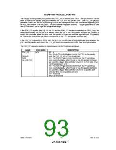
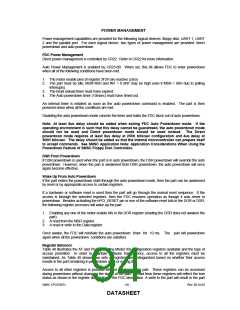
FLOPPY ON PARALLEL PORT PIN
The “floppy on the parallel port” pin function, FDC_PP, is muxed onto GP43. This pin function can be
used to switch the parallel port pins between the FDC and the parallel port. The FDC_PP pin can
generate a PME and an SMI by enabling GP43 in the appropriate PME and SMI enable registers (bit 5
of PME_EN4 and bit 6 of SMI_EN4 – see the Runtime Registers section). This pin generates an SMI
and SCI on both a low-to-high and a high-to-low edge.
If the FDC_PP register bits[1:0] =01 or 10, and the FDC_PP function is selected on GP43, then the
default functionality for this pin is as follows: when the pin is low, the parallel port pins are used for a
floppy disk controller; when the pin is high, the parallel port pins are used for a parallel port. The polarity
bit controls the state of the pin, which corresponds to the FDC and parallel port function.
If the FDC_PP register bits[1:0]=00 then the pin is not used to switch the parallel port pins between the
FDC and the parallel port, even if the FDC_PP function is selected on GP43. See description below.
The FDC_PP register is located in logical device A at 0xF1 defined as follows:
NAME
REG INDEX
0xF1
DESCRIPTION
FDC_PP
Bit[1:0]
00 = Bits in PP mode Register control the FDC on the parallel
port, the FDC_PP pin function is not used.
Default =
0x00
01 = The FDC_PP pin controls the FDC on the PP as follows:
(non-inverted polarity) when the pin is low, the parallel port pins
are used for a floppy disk controller: drive 0 is on FDC pins, drive
1 is on parallel port pins
on VTR POR
10 = The FDC_PP pin controls the FDC on the PP as follows:
(non-inverted polarity) when the pin is low, the parallel port pins
are used for a floppy disk controller: drive 0 is on parallel port
pins and drive 1 is on parallel port pins
11 = Reserved
Bits[7:2] Reserved
SMSC LPC47B27x
- 93 -
Rev. 08-10-04
DATASHEET

 SMSC [ SMSC CORPORATION ]