PARALLEL PORT FLOPPY DISK CONTROLLER
The Floppy Disk Control signals are available optionally on the parallel port pins. When this mode is
selected, the parallel port is not available. There are two modes of operation, PPFD1 and PPFD2. These
modes can be selected in the Parallel Port Mode Register, as defined in the Parallel Port Mode Register,
Logical Device 3, at 0xF1. PPFD1 has only drive 1 on the parallel port pins; PPFD2 has drive 0 and 1 on
the parallel port pins. The FDC_PP pin can be used to switch the parallel port pins between the FDC and
the parallel port functions. See the following section.
FDC SWAP BIT
The FDC_SWAP bit in the FDD Mode Register (configuration register 0xF0) can be used to swap (nDS0,
nMTR0) and (nDS1, nMTR1) pins. This applies to both PPFD1 and PPFDC2 modes. The FDC_SWAP is
defined as follows:
Bit[4] FDC_SWAP
0 = Do Not Swap (default)
1 = Swap Drive 0 (nDS, nMTR pins) with Drive 1 (nDS , nMTR pins)
Mode
FDC_SWAP Description
PPFD1
0
1
0
1
Drive 0 on FDC
Drive 1 on PP
Drive 1 on FDC
Drive 0 on PP
PPFD2
Both Drives on PP.
Don’t swap
Both Drives on PP.
Swap Drives 0 and 1
The following parallel port pins are read as follows by a read of the parallel port register:
1. Data Register (read) = last Data Register (write)
2. Control Register read as "cable not connected" STROBE, AUTOFD and SLC = 0 and nINIT =1
3. Status Register reads: nBUSY = 0, PE = 0, SLCT = 0, nACK = 1, nERR = 1
The following FDC pins are all in the high impedence state when the PPFDx is actually selected by the PP
Mode Register 2:
1) nWDATA, nHDSEL, nWGATE, nDIR, nSTEP, nDS0, nMTR0 outputs are used when PPFD2 is
selected. The DRVDEN0, DRVDEN1, nDS1, and nMTR1 pins should be configured as GPIO or
other functions if PPFD2 is selected.
2) nDS1 and nMTR1 should configured as GPIO or other functions when PPFD1 is selected.
3) All unused inputs and outputs should be externally pulled-up.
4) If PPFDx is selected, then the parallel port can not be used as a parallel port until "Normal" mode is
selected.
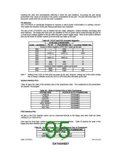
The FDC signals are muxed onto the Parallel Port pins as shown in Table 46.
For ACPI compliance the FDD pins that are multiplexed onto the Parallel Port function independently of
the state of the Parallel Port controller. For example, if the FDC is enabled onto the Parallel Port the
multiplexed FDD interface functions normally regardless of the Parallel Port Power control, CR22.3.
Table 46 illustrates this functionality.
TABLE 46 - MODIFIED PARALLEL PORT FDD CONTROL
PARALLEL
PARALLEL PORT FDC
CONTROL
PARALLEL PORT
FDC STATE
PARALLEL PORT
STATE
PORT
POWER
CR22.3
LD3:CRF1.1
LD3:CRF1.0
1
0
X
0
0
1
X
0
0
X
1
OFF
OFF
ON
ON
OFF
OFF
(NOTE1)
SMSC LPC47B27x
- 91 -
Rev. 08-10-04
DATASHEET

 SMSC [ SMSC CORPORATION ]