(3) = High Speed Mode
Note:
For the cable interconnection required for ECP support and the Slave Connector pin numbers,
refer to the IEEE 1284 Extended Capabilities Port Protocol and ISA Standard, Rev. 1.14, July 14, 1993.
This document is available from Microsoft.
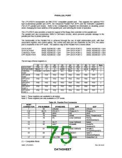
IBM XT/AT COMPATIBLE, BI-DIRECTIONAL AND EPP MODES
DATA PORT
ADDRESS OFFSET = 00H
The Data Port is located at an offset of '00H' from the base address. The data register is cleared at
initialization by RESET. During a WRITE operation, the Data Register latches the contents of the internal
data bus. The contents of this register are buffered (non inverting) and output onto the PD0 - PD7 ports.
During a READ operation in SPP mode, PD0 - PD7 ports are buffered (not latched) and output to the host
CPU.
STATUS PORT
ADDRESS OFFSET = 01H
The Status Port is located at an offset of '01H' from the base address. The contents of this register are
latched for the duration of a read cycle. The bits of the Status Port are defined as follows:
BIT 0 TMOUT - TIME OUT
This bit is valid in EPP mode only and indicates that a 10 usec time out has occurred on the EPP bus. A
logic O means that no time out error has occurred; a logic 1 means that a time out error has been
detected. This bit is cleared by a RESET. Writing a one to this bit clears the time out status bit. On a
write, this bit is self clearing and does not require a write of a zero. Writing a zero to this bit has no effect.
BITS 1, 2 - are not implemented as register bits, during a read of the Printer Status Register these bits are
a low level.
BIT 3 nERR - nERROR
The level on the nERROR input is read by the CPU as bit 3 of the Printer Status Register. A logic 0
means an error has been detected; a logic 1 means no error has been detected.
BIT 4 SLCT - PRINTER SELECTED STATUS
The level on the SLCT input is read by the CPU as bit 4 of the Printer Status Register. A logic 1 means
the printer is on line; a logic 0 means it is not selected.
BIT 5 PE - PAPER END
The level on the PE input is read by the CPU as bit 5 of the Printer Status Register. A logic 1 indicates a
paper end; a logic 0 indicates the presence of paper.
BIT 6 nACK - nACKNOWLEDGE
The level on the nACK input is read by the CPU as bit 6 of the Printer Status Register. A logic 0 means
that the printer has received a character and can now accept another. A logic 1 means that it is still
processing the last character or has not received the data.
BIT 7 nBUSY - nBUSY
The complement of the level on the BUSY input is read by the CPU as bit 7 of the Printer Status Register.
A logic 0 in this bit means that the printer is busy and cannot accept a new character. A logic 1 means that
it is ready to accept the next character.
CONTROL PORT
ADDRESS OFFSET = 02H
The Control Port is located at an offset of '02H' from the base address. The Control Register is initialized
by the RESET input, bits 0 to 5 only being affected; bits 6 and 7 are hard wired low.
BIT 0 STROBE - STROBE
This bit is inverted and output onto the nSTROBE output.
SMSC LPC47B27x
- 76 -
Rev. 08-10-04
DATASHEET

 SMSC [ SMSC CORPORATION ]