FUNCTIONAL DESCRIPTION
SUPER I/O REGISTERS
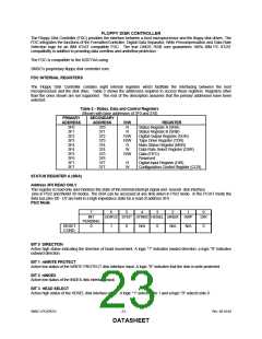
The address map, shown below in Table 1, shows the addresses of the different blocks of the Super I/O immediately
after power up. The base addresses of the FDC, serial and parallel ports, PME register block, Game port and
configuration register block can be moved via the configuration registers. Some addresses are used to access more
than one register.
HOST PROCESSOR INTERFACE (LPC)
The host processor communicates with the LPC47B27x through a series of read/write registers via the LPC interface.
The port addresses for these registers are shown in Table 1. Register access is accomplished through I/O cycles or
DMA transfers. All registers are 8 bits wide.
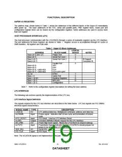
Table 1 - Super I/O Block Addresses
LOGICAL
ADDRESS
Base+(0-5) and +(7)
Base+(0-7)
BLOCK NAME
Floppy Disk
DEVICE
NOTES
0
4
5
Serial Port Com 1
Serial Port Com 2
Base1+(0-7)
IR Support
Base2+(0-7)
Consumer IR
Parallel Port
SPP
3
Base+(0-3)
Base+(0-7)
EPP
Base+(0-3), +(400-402)
Base+(0-7), +(400-402)
60, 64
ECP
ECP+EPP+SPP
KYBD
7
9
A
B
Base + 0
Game Port
Runtime Registers
MPU-401
Configuration
Base + (0-5F)
Base + (0-1)
Base + (0-1)
Note 1: Refer to the configuration register descriptions for setting the base address.
LPC INTERFACE
The following sub-sections specify the implementation of the LPC bus.
LPC Interface Signal Definition
The signals required for the LPC bus interface are described in the table below. LPC bus signals use PCI 33MHz
electrical signal characteristics.
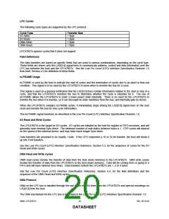
SIGNAL NAME
LAD[3:0]
TYPE
DESCRIPTION
LPC address/data bus. Multiplexed command, address and data bus.
Frame signal. Indicates start of new cycle and termination of broken
cycle
I/O
nLFRAME
Input
nPCI_RESET
nLDRQ
nIO_PME
nLPCPD
Input
PCI Reset. Used as LPC Interface Reset.
Output Encoded DMA/Bus Master request for the LPC interface.
OD
Input
Power Mgt Event signal. Allows the LPC47B27x to request wakeup.
Powerdown Signal. Indicates that the LPC47B27x should prepare for
power to be shut on the LPC interface.
Serial IRQ.
SER_IRQ
PCI_CLK
I/O
Input
PCI Clock.
Note: The nCLKRUN signal is not implemented in this part.
SMSC LPC47B27x
- 19 -
Rev. 08-10-04
DATASHEET

 SMSC [ SMSC CORPORATION ]