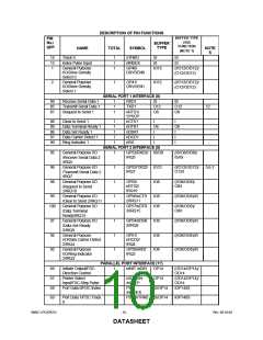
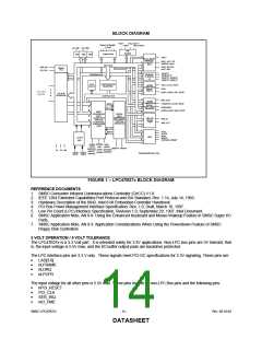
BLOCK DIAGRAM
FAN_TACH1*
FAN2* FAN_TACH2*
FAN1*
Game Port Signals*
(1-Dual)
nIO_SMI nIO_PME
...
Fan
Control
Game Port
DATA BUS
SMI
PME
WDT
PD0-7
MULTI-MODE
PARALLEL
PORT/FDC
MUX
BUSY, SLCT, PE,
nERROR, nACK
nSTB, nSLCTIN,
nINIT, nALF
SER_IRQ
PCI_CLK
SERIAL
IRQ
GP1[0:7]*
ADDRESS BUS
GENERAL
PURPOSE
I/O
GP2[0:2,4:7]*
GP3[0:7]*, GP4[0:3]*
GP5[0:7]*, GP6[0:1]*
ACPI
CONFIGURATION
REGISTERS
TXD1, nCTS1, nRTS1
RXD1
16C550
COMPATIBLE
SERIAL
BLOCK
PORT 1
LPC Bus
Signals
nDSR1, nDCD1, nRI1, nDTR1
LPC BUS
INTERFACE
CONTROL BUS
IRRX, IRTX
TXD2(IRTX), nCTS2, nRTS2*
16C550
COMPATIBLE
SERIAL
WDATA
RXD2(IRRX)*
nDSR2, nDCD2, nRI2, nDTR2*
PORT 2 WITH
INFRARED
WCLOCK
SMSC
PROPRIETARY
82077
DIGITAL
DATA
SEPARATOR
WITH WRITE
PRECOM-
COMPATIBLE
VERTICAL
MPU-401
SERIAL
PORT
MIDI_IN
FLOPPYDISK
CONTROLLER
CORE
MIDI_OUT
PENSATION
RCLOCK
RDATA
KCLK
KDATA
MCLK
8042
CLOCK
GEN
MDATA
GATEA20, KRESET
DENSEL
nDIR nMTR0
nINDEX
nTRK0
nDS0
nWDATA nRDATA
nDSKCHG
nWRPRT
nWGATE
14MHz
nSTEP DRVDEN0
VTR Vcc Vss
*
DRVDEN1
nHDSEL
*
CLK32 CLOCKI
Denotes Multifunction Pins
32KHz
FIGURE 1 – LPC47B27x BLOCK DIAGRAM
REFERENCE DOCUMENTS
1. SMSC Consumer Infrared Communications Controller (CIrCC) V1.X
2. IEEE 1284 Extended Capabilities Port Protocol and ISA Standard, Rev. 1.14, July 14, 1993.
3. Hardware Description of the 8042, Intel 8 bit Embedded Controller Handbook.
4. PCI Bus Power Management Interface Specification, Rev. 1.0, Draft, March 18, 1997.
5. Low Pin Count (LPC) Interface Specification, Revision 1.0, September 29, 1997, Intel Document.
6. SMSC Application Note, AN 8-8: Using the Enhanced Keyboard and Mouse Wakeup Feature in SMSC Super I/O
Parts.
7. SMSC Application Note, AN 9-3: Application Considerations When Using the Powerdown Feature of SMSC
Floppy Disk Controllers.
3 VOLT OPERATION / 5 VOLT TOLERANCE
The LPC47B27x is a 3.3 Volt part. It is intended solely for 3.3V applications. Non-LPC bus pins are 5V tolerant; that
is, the input voltage is 5.5V max, and the I/O buffer output pads are backdrive protected.
The LPC interface pins are 3.3 V only. These signals meet PCI DC specifications for 3.3V signaling. These pins are:
•
•
•
•
LAD[3:0]
nLFRAME
nLDRQ
nLPCPD
The input voltage for all other pins is 5.5V max. These pins include all non-LPC Bus pins and the following pins:
•
•
•
•
nPCI_RESET
PCI_CLK
SER_IRQ
nIO_PME
SMSC LPC47B27x
- 14 -
Rev. 08-10-04
DATASHEET

 SMSC [ SMSC CORPORATION ]