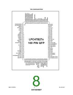
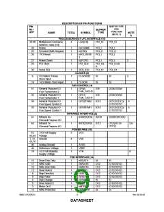
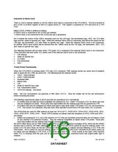
DESCRIPTION OF PIN FUNCTIONS
BUFFER TYPE
PER
PIN
No./
QFP
BUFFER
TYPE
FUNCTION
(NOTE 1)
NAME
TOTAL
SYMBOL
NOTE
S
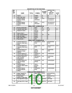
41
42
General Purpose I/O /
P17
1
1
GP20/P17
IO8
(I/O8/OD8)/
IO8
(I/O12/OD12)/
IO12/(O12/
OD12)
General Purpose I/O /
GP21 /P16/
nDS1
IO12
IO12
P16 /nDS1
43
General Purpose I/O /
P12/nMTR1
1
GP22 /P12/
nMTR1
(I/O12/
OD12)/IO12/
(O12/OD12)
45
46
47
50
48
49
17
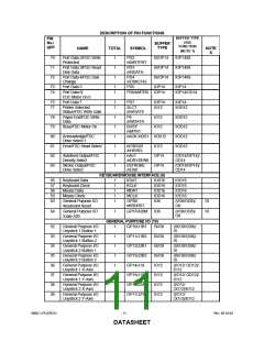
General Purpose I/O /
System Option
1
1
1
1
1
1
1
GP24
IO8
(I/O8/OD8)
9
/SYSOPT
General Purpose I/O
GP25
IO8
(I/O8/OD8)/I
/MIDI_IN
/MIDI_IN
General Purpose I/O
/MIDI_OUT
GP26
IO12
IO12
(I/O12/OD12)/
O12
/MIDI_OUT
General Purpose I/O
/SMI Output
GP27
(I/O12/OD12)/
/nIO_SMI
OD12
General Purpose I/O /
GP60 /LED1 IO12
(I/O12/OD12)/
O12
11
11
LED
General Purpose I/O /
LED
GP61 /LED2 IO12
(I/O12/OD12)/
O12
General Purpose I/O /
Power Management
Event
General Purpose I/O
/Device Disable Reg.
Control / FDC on
Parallel Port
GP42
IO12
(I/O12/OD12)/
OD12
/nIO_PME
28
1
GP43/DDRC IO8
/FDC_PP
(I/O8/OD8)/I/I
Note:
The "n" as the first letter of a signal name indicates an "Active Low" signal.
Note 1: Buffer types per function on multiplexed pins are separated by a slash “/”. Buffer types in parenthesis
represent multiple buffer types for a single pin function.
Note 2: The nLPCPD pin may be tied high. The LPC interface will function properly if the nPCI_RESET signal
follows the protocol defined for the nLRESET signal in the “Low Pin Count Interface Specification”.
Note 3: If the 32kHz input clock is not used the CLKI32 pin must be grounded. There is a bit in the configuration
register at 0xF0 in Logical Device A that indicates whether or not the 32kHz clock is connected. This bit
determines the clock source for the fan tachometer, LED and “wake on specific key” logic. Set this bit to ‘1’
if the clock is not connected.
Note 4. The fan control pins (FAN1 and FAN2) come up as outputs and low following a VCC POR and Hard Reset.
Note 5: The IRTX pins (IRTX2/GP35 and GP53/TXD2) are driven low when the part is powered by VTR (VCC=0V
with VTR=3.3V). The IRTX2/GP35 pin will remain low following a power-up (VCC POR) until serial port 2 is
enabled by setting the activate bit, at which time the pin will reflect the state of the IR transmit output of the
IRCC block. The GP53/TXD2 pin will remain low following a VCC POR until the TXD2 function is selected
for the pin and serial port is enabled by setting the activate bit, at which time the pin will reflect the state of
the IR transmit output of the IRCC block (if IR is enabled).
Note 6:The “activate” bit for the CIrCC is reset by VTR POR only. The VCC power-up default for this pin is Logic “0” if the
IRTX2 function is programmed on the GPIO.
Note 7:The “activate” bit for Serial Port 2 is reset by VTR POR only. The VCC power-up default for this pin is Logic “0” if
the TXD2 function is programmed on the GPIO.
Note 8: VTR can be connected to VCC if no wakeup functionality is required.
Note 9: The GP24 /SYSOPT pin requires an external pulldown resistor to put the base IO address for configuration
at 0x02E. An external pullup resistor is required to move the base IO address for configuration to 0x04E.
Note 10: External pullups must be placed on the nKBDRST and A20M pins. These pins are GPIOs that are inputs
after an initial power-up (VTR POR). If the nKBDRST and A20M functions are to be used, the system must
ensure that these pins are high. See Section “Pins That Require External Pullup Resistor”.
Note 11: The LED pins are powered by VTR so that the LEDs can be controlled when the part is under VTR power
SMSC LPC47B27x
- 12 -
Rev. 08-10-04
DATASHEET

 SMSC [ SMSC CORPORATION ]