Three Port 10/100 Managed Ethernet Switch with MII
Datasheet
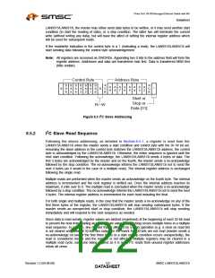
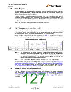
Note 9.1 PHY Address bit 4 is 1 for SMI commands. PHY Address 3:0 form system register address
bits 9:6. The Register Address field forms the system register address bits 5:1
Note 9.2 The turn-around time (TA) is used to avoid contention during a read cycle. For a read, the
LAN9313/LAN9313i drives the second bit of the turn-around time to 0, and then drives the
msb of the read data in the following clock cycle. For a write, the external host drives the
first bit of the turn-around time to 1, the second bit of the turn-around time to 0, and then
the msb of the write data in the following clock cycle.
Note 9.3 In the IDLE condition, the MDIO output is three-stated and pulled high externally.
Note: The SMI interface supports up to a 2.5MHz input clock. The MII/SMI timing adheres to the
IEEE 802.3 specification. Refer to the IEEE 802.3 specification for detailed MII timing
information.
9.2.1
Read Sequence
In a read sequence, the host sends the 32-bit preamble, 2-bit start of frame, 2-bit op-code, 5-bit PHY
Address, and the 5-bit Register Address. The next clock is the first bit of the turnaround time in which
the LAN9313/LAN9313i continues to three-state MDIO. On the next rising edge of MDC, the
LAN9313/LAN9313i drives MDIO low. For the next 16 rising edges, the LAN9313/LAN9313i drives the
output data. On the final clock, the LAN9313/LAN9313i once again three-states MDIO.
The host processor is required to perform two consecutive 16-bit reads to complete a single DWORD
transfer. No ordering requirements exist. The processor can access either the low or high word first,
as long as the next read is performed from the other word. If a read to the same word is performed,
the combined data read pair is invalid and should be re-read. This is not a fatal error. The
LAN9313/LAN9313i will simply reset the read counters, and restart a new cycle on the next read.
Note: Select registers are readable as 16-bit registers, as noted in their register descriptions. For
these registers, only one 16-bit read may be performed without the need to read the other
word.
Register values are latched (registered) at the beginning of each 16-bit read to prevent the host from
reading an intermediate value. In addition, any register that is affected by a read operation, such as a
clear on read bit, is not cleared until after the end of the second read. In the event that 32-bits are not
read, the read in considered invalid and the register is not affected.
Any register that may change between two consecutive host read cycles and spans across two
WORDs, such as a counter, is latched (registered) at the beginning of the first read and held until after
the second read has completed. This prevents the host from reading inconsistent data from the first
and second half of a register. For example, if a counters value is 01FFh, the first half will be read as
01h. If the counter then changes to 0200h, the host would read 00h, resulting an the incorrect value
of 0100h instead of either 01FFh or 0200h.
Note: SMI reads from unused register addresses return all zeros. This differs from unused PHY
registers which leave MDIO un-driven.
9.2.1.1
SMI Read Polling for Reset Complete
During reset, the SMI slave interface will not return valid data. To determine when the reset condition
is complete, the Byte Order Test Register (BYTE_TEST) should be polled. Once the correct pattern is
read, the interface can be considered functional. At this point, the READY bit in the Hardware
Configuration Register (HW_CFG) can be polled to determine when the device initialization is
complete. Refer to Section 4.2, "Resets," on page 41 for additional information.
Note: In the event that a reset condition terminates between halves of 16-bit read pair, the
LAN9313/LAN9313i will not expect another 16-bit read to complete the DWORD cycle. Only
specific registers may be read during a reset. Refer to Section 4.2, "Resets," on page 41 for
additional information.
Revision 1.2 (04-08-08)
126
SMSC LAN9313/LAN9313i
DATASHEET

 SMSC [ SMSC CORPORATION ]