Non-PCI Single-Chip Full Duplex Ethernet Controller with Magic Packet
The data path routed by the arbiter goes between memory (the data path does not go through the MMU)
on one side and either the CPU side bus or the data path of the CSMA/CD core.
The data path between memory and the Data Register is in fact buffered by a small FIFO in each direction.
The FIFOs beneath the Data Register can be read and written as bytes or words, in any sequential
combination. The presence of these FIFOs makes sure that word transfers are possible on the system bus
even if the address loaded into the pointer is odd.
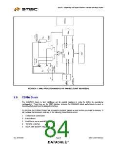
9.3
Bus Interface
The bus interface handles the data, address and control interfaces and is compliant with the LOCAL BUS,
PCMCIA, and 68000-interface specifications and allows 8 or 16 bit adapters to be designed with the
LAN91C96 with no glue to interface the LOCAL BUS or PCMCIA bus.
The functions in this block include address decoding for I/O and ROM memory (including address
relocation support) for LOCAL BUS, data path routing, sequential memory address support, optional wait
state generation, boot ROM support, EEPROM setup function, bus transceiver control, and interrupt
generation / selection.
For LOCAL BUS, I/O address decoding is done by comparing A15-A4 to the I/O BASE address
determined in part by the upper byte of the BASE ADDRESS REGISTER, and also requiring that AEN be
low. If the above address comparison is satisfied and the LAN91C96 is in 16 bit mode, nIOCS16 will be
asserted (low).
A valid comparison does not yet indicate a valid I/O cycle is in progress, as the addresses could be used
for a memory cycle, or could even glitch through a valid value. For LOCAL BUS and PCMCIA, only
when nIORD or nIOWR are activated the I/O cycle begins.
In PCMCIA mode, A4-A15 are ignored for I/O decodes, which rely on the PCMCIA host, decoding for the
slot. Input A10 for LOCAL BUS is used as an output (nFWE) for PCMCIA to enable Flash Memory Write
for programming the attribute memory. It is valid only when nWE is “0” and COR2 is “1”. nA11/nFCS is
used to select the Flash Memory Chip.
The LAN91C96 provides a glueless interface to a stripped down version of the Motorola 68000 processor.
This interface is limited to 16 bits only. None of the size or function pins are supported. The LAN91C96
functions as a slave and requires some of its pins pulled high or low for the interface to function.
The SMC91C96 enters the 68000 interface mode when nIORD and nIOWR are asserted simultaneously.
Once the two are asserted together, the only way to return to the LOCAL BUS interface is by hard
resetting the chip. Notice that the chip is required to power up in LOCAL BUS mode to use the 68000
interface.
For the first chip access, the first transfer (to the 91C96) must be a write as the controller uses this write to
confirm the 68000 mode. The LAN91C96 responds to addresses per the base address register contents
(as in the LOCAL BUS mode).
9.4
Wait State Policy
The LAN91C96 can work on most system buses without having to add wait states. The two parameters
that determine the memory access profile are the read access time and the cycle time into the Data
Register.
The read access time is 40ns and the cycle time is 185ns. If any one of them does not satisfy the
application requirements, wait states should be added.
Rev. 09/10/2004
Page 80
SMSC LAN91C965v&3v
DATASHEET

 SMSC [ SMSC CORPORATION ]