Non-PCI Single-Chip Full Duplex Ethernet Controller with Magic Packet
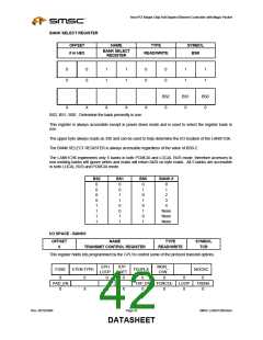
BANK SELECT REGISTER
OFFSET
# in HEX
NAME
TYPE
SYMBOL
BSR
BANK SELECT
READ/WRITE
REGISTER
0
0
0
0
1
1
1
1
0
0
0
0
1
1
1
1
BS2
0
BS1
0
BS0
0
X
X
X
X
X
BS2, BS1, BS0 - Determine the bank presently in use.
This register is always accessible except in power down mode and is used to select the register bank in
use.
The upper byte always reads as 33h and can be used to help determine the I/O location of the LAN91C96.
The BANK SELECT REGISTER is always accessible regardless of the value of BS0-2.
The LAN91C96 implements only 5 banks in both PCMCIA and LOCAL BUS mode, therefore accesses to
non-existing banks will ignore writes and reads will return 0x33 on byte reads. All 5 banks are accessible
in both LOCAL BUS and PCMCIA mode.
BS2
0
BS1
0
BS0
0
BANK #
0
1
0
0
1
0
1
0
2
0
1
1
3
1
0
0
4
1
0
1
None
None
None
1
1
0
1
1
1
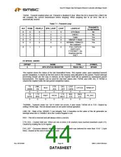
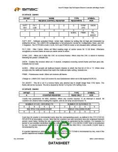
I/O SPACE - BANK0
OFFSET
0
NAME
TRANSMIT CONTROL REGISTER
TYPE
READ/WRITE
SYMBOL
TCR
This register holds bits programmed by the CPU to control some of the protocol transmit options.
EPH
LOOP
0
STP
SQET
0
MON_
FDSE
ETEN-TYPE
0
FDUPLX
NOCRC
CSN
0
PAD_EN
0
0
TXP_EN
0
0
FORCOL
0
X
LOOP
0
0
TXENA
0
X
X
X
Rev. 09/10/2004
Page 42
SMSC LAN91C965v&3v
DATASHEET

 SMSC [ SMSC CORPORATION ]