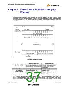
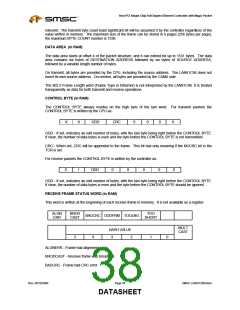
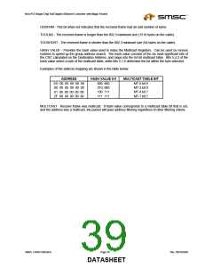
Non-PCI Single-Chip Full Duplex Ethernet Controller with Magic Packet
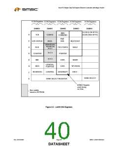
Chapter 7 Registers Map in I/O Space
7.1
I/O Space Access
The address is determined by the Ethernet I/O Base Registers. The Ethernet I/O space can be configured
as an 8 or 16 bit I/O space, and is similar to the LAN91C94, LAN91C92, etc. I/O space mapping. To limit
the I/O space requirements to 16 locations, the registers are Split into 4 banks in LOCAL BUS mode and 5
banks in PCMCIA mode. The last word of the I/O area is shared by all banks and can be used to change
the bank in use. Banks 0 through 3 functionally correspond to the LAN91C94 banks, while Bank 4 allows
access to the PCMCIA registers in LOCAL BUS mode.
Registers are described using the following convention:
OFFSET
NAME
TYPE
SYMBOL
BSR
BANK SELECT
REGISTER
E
READ/WRITE
BIT 15
BIT14
BIT 13
BIT 12
BIT 11
BIT 10
BIT9
BIT8
RST
RST
RST
RST
RST
RST
RST
RST
Val
Val
Val
Val
Val
Val
Val
Val
BIT 7
BIT 6
BIT 5
BIT 4
BIT 3
BIT 2
BIT 1
BIT 0
RST
RST
RST
RST
RST
RST
RST
RST
Val
Val
Val
Val
Val
Val
Val
Val
OFFSET - Defines the address offset within the IOBASE where the register can be accessed at, provided
the bank select has the appropriate value. The offset specifies the address of the even byte (bits 0-7) or
the address of the complete word. The odd byte can be accessed using address (offset + 1).
Some registers (e.g. the Interrupt Ack. or the Interrupt Mask) are functionally described as two eight bit
registers. In such case, the offset of each one is independently specified.
Regardless of the functional description, when the LAN91C96 is in 16 bit mode, all registers can be
accessed as words or bytes.
RST Val - The default bit values upon hard reset are highlighted below each register.
7.2
I/O Space Registers Description
(Bank 4 Registers are described under PCMCIA Configuration Registers and will not be described again).
SMSC LAN91C965v&3v
Page 41
Rev. 09/10/2004
DATASHEET

 SMSC [ SMSC CORPORATION ]