been initialized to 01H. The default value of this
register after power up is 9CH.
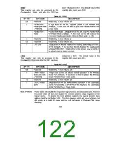
CR01
This register can only be accessed in the
Configuration Mode and after the CSR has
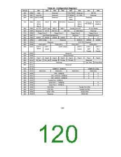
Table 48 - CR01
BIT NO.
BIT NAME
Reserved
Parallel Port
Power (see note (Default). A low level on this bit puts the Parallel Port in low
DESCRIPTION
Read Only. A read returns a 0.
A high level on this bit, supplies power to the Parallel Port
0,1
2
_PWRDN)
power mode.
3
Parallel Port
Mode
Parallel Port Mode. A high level on this bit, sets the Parallel Port
for Printer Mode (Default). A low level on this bit enables the
Extended Parallel port modes. Refer to Bits 0 and 1 of CR4
4
5,6
7
Reserved
Reserved
Lock CRx
Read Only. A read returns a 1.
Read Only. A read returns a 0.
A high level on this bit enables the reading and writing of CR00-
CR18 (Default). A low level on this bit disables the reading and
writing of CR0-CRF. Once set to 0, this bit can only be set to 1
by a hard reset or power-up reset.
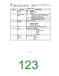
initialized to 02H. The default value of this
CR02
This register can only be accessed in the
register after power up is 88H.
Configuration Mode and after the CSR has been
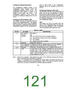
Table 49 - CR02
BIT NO.
BIT NAME
Reserved
DESCRIPTION
0:2
3
Read Only. A read returns a 0.
UART1 Power
down (see note
_PWRDN)
A high level on this bit, allows normal operation of the Primary
Serial Port (Default). A low level on this bit places the Primary
Serial Port into Power Down Mode.
4:6
7
Reserved
Read Only. A read returns a 0.
UART2 Power
down
A high level on this bit, allows normal operation of the Secondary
Serial Port (Default). A low level on this bit places the Secondary
Serial Port into Power Down Mode.
Note_PWRDN: Power Down bits disable the respective logical device and associated pins, however
the power down bit does not disable the selected address range registers for the
logical device. To disable the host address registers the logical device's base
address must be set below 100h. Therefore devices which are powered down, but
still reside at a valid I/O base address will participate in Plug-and-Play range
checking.
122

 SMSC [ SMSC CORPORATION ]