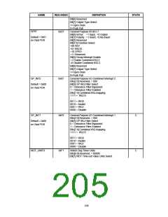
ACPI, Logical Device A
TABLE 85 - ACPI, LOGICAL DEVICE A [LOGICAL DEVICE NUMBER = 0X0A]
NAME
REG INDEX
DEFINITION
STATE
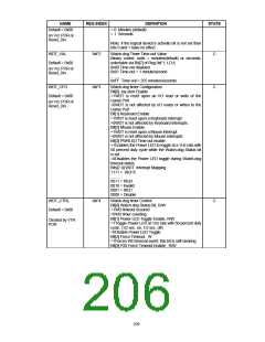
Sleep/Wake
Configuration
This register is used to configure the functionality of
the SLP_EN bit and its associated logic, and the
WAK_STS bit bit and its associated logic. It also
contains the CIR PLL Power bit.
0xF0
C
Default = 0x00
on Vbat POR
Bit[0] SLP_CTRL. SLP_EN Bit Function.
0=Default. Writing ‘1’ to the SLP_EN bit causes the
system to sequence into the sleeping state associated
with the SLP_TYPx fields.
1=Writing ‘1’ to the SLP_EN bit does not cause the
system to sequence into the sleeping state associated
with the SLP_TYPx fields; instead an SMI is
generated.
Note: the SLP_EN_SMI bit in the SMI Status Register
2 is set whenever ‘1’ is written to the SLP_EN bit; it is
enabled to generate an SMI through bit[0] of this
register.
Bit[1] WAK_CTRL. WAK_STS Bit Function
0=Default. The WAK_STS bit is set on the high-to-low
transition of nPowerOn.
1=The WAK_STS bit is set upon any enabled wakeup
event and the high-to-low transition of nPowerOn.
Bits[2:6] Reserved
Bit[7]: CIR PLL Power.
0=Default. The 32KHz clock PLL is unpowered
1=The 32KHz clock PLL is running and can replace
the 14.318MHz clock source for the CIR wakeup
event.
212

 SMSC [ SMSC CORPORATION ]