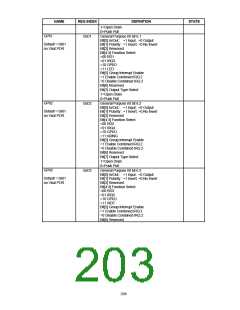
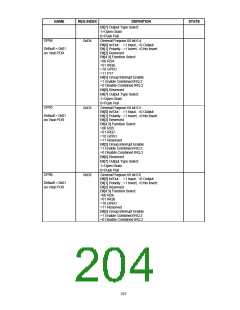
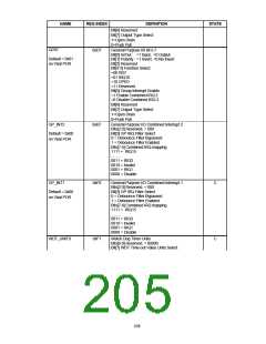
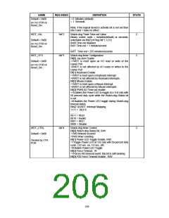
NAME
REG INDEX
DEFINITION
STATE
= 1Allows rising edge of P20, from the Keyboard
Controller, to force the WD timeout event. A WD
timeout event may still be forced by setting the Force
Timeout Bit, bit 2.
= 0P20 activity does not generate the WD timeout
event.
Note: The P20 signal will remain high for a minimum
of 1us and can remain high indefinitely. Therefore,
when P20 forced timeouts are enabled, a self-clearing
edge-detect circuit is used to generate a signal which
is ORed with the signal generated by the Force
Timeout Bit.
Bit[4] Reserved. Set to 0.
Bit[5] Stop_Cnt: This is used to terminate Delay 2
(Note 1) without generating a power down. This is
used if the software determines that the power down
should be aborted. When read, this bit indicates the
following: Stop_Cnt = 0; Counter running Stop_Cnt
= 1; Counter Stopped. Note: The write is self
clearing.
Bit[6] Restart_Cnt: This is used to restart Delay 2
(Note 1) from the button input to the generation of
the power down. When restarted, the count will start
over and delay the power down for the time that
Delay 2 is set for (Default=500msec). The software
can continue to do this indefinately with out allowing
a powerdown. This bit is self clearing. 1=Restart;
Automatically cleared.
Bit[7] SPOFF: This is used to force a software
power down. This bit is self clearing.
Note 1: This delay is programmable via the Delay 2
Time Set Register at Logical Device 8, 0xB8.
GP1
0xF6
This register is used to read the value of the GPIO
pins.
Default = 0x00
on Vbat POR
Bit[0]: GP10
Bit[1]: GP11
Bit[2]: GP12
Bit[3]: GP13
Bit[4]: GP14
Bit[5]: GP15
Bit[6]: GP16
Bit[7]: GP17
GP5
0xF9
This register is used to read the value of the GPIO
pins.
Bit[0]: GP50
Bit[1]: Reserved
Bit[2]: GP52
Default = 0x00
on Vbat POR
210

 SMSC [ SMSC CORPORATION ]