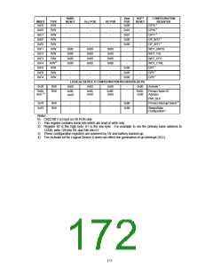
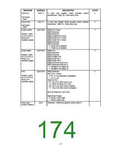
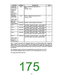
Logical Device Configuration/Control Registers [0x30-0xFF]
Used to access the registers that are assigned to each logical unit. This chip supports eight logical units
and has eight sets of logical device registers. The eight logical devices are Floppy, Parallel Port, Serial
Port 1 and Serial Port 2, Real Time Clock, Keyboard Controller, Auxiliary I/O and ACPI. A separate set
(bank) of control and configuration register exists for each logical device and is selected with the Logical
Device # Register (0x07).
The INDEX PORT is used to select a specific logical device register. These registers are then accessed
through the DATA PORT.
The Logical Device registers are accessible only when the device is in the Configuration State. The logical
register addresses are:
Logical Device Registers
TABLE 72 - CHIP LEVEL REGISTERS
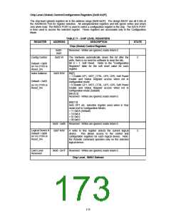
LOGICAL DEVICE
REGISTER
Activate Note1
ADDRESS
DESCRIPTION
STATE
(0x30)
Bits[7:1] Reserved, set to zero.
C
Bit[0]
Default = 0x00
= 1 Activates the logical device currently selected
through the Logical Device # register.
= 0 Logical device currently selected is inactive
on Vcc POR or
Reset_Drv Note 2
Logical Device
Control
(0x31-0x37) Reserved - Writes are ignored, reads return 0.
C
C
Logical Device
Control
(0x38-0x3f) Vendor Defined - Reserved - Writes are ignored,
reads return 0.
Mem Base Addr
I/O Base Addr.
(0x40-0x5F) Reserved - Writes are ignored, reads return 0.
C
C
(0x60-0x6F) Registers 0x60 and 0x61 set the base address for the
device. If more than one base address is required,
(see Device Base I/O
Address Table)
0x60,2,... = the second base address is set by registers 0x62 and
addr[15:8]
0x63.
Unused registers will ignore writes and return zero
when read.
Default = 0x00
0x61,3,... =
addr[7:0]
on Vcc POR or
Reset_Drv
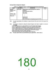
Interrupt Select
(0x70,072)
0x70 is implemented for each logical device. Refer to
Interrupt Configuration Register description. Only the
keyboard controller uses Interrupt Select register
0x72. Unused register (0x72) will ignore writes and
return zero when read. Interrupts default to edge high
(ISA compatible).
C
Defaults :
0x70 = 0x00,
on Vcc POR or
Reset_Drv
0x72 = 0x00,
on Vcc POR or
Reset_Drv
179

 SMSC [ SMSC CORPORATION ]