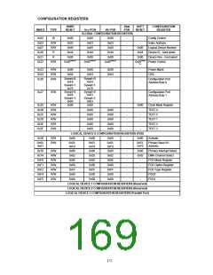
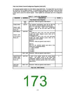
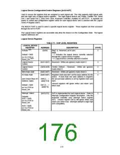
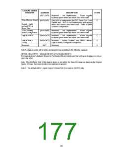
Chip Level (Global) Control/Configuration Registers [0x00-0x2F]
The chip-level (global) registers lie in the address range [0x00-0x2F]. The design MUST use all 8 bits of
the ADDRESS Port for register selection. All unimplemented registers and bits ignore writes and return
zero when read. The INDEX PORT is used to select a configuration register in the chip. The DATA PORT
is then used to access the selected register. These registers are accessable only in the Configuration
Mode.
TABLE 71 - CHIP LEVEL REGISTERS
REGISTER
ADDRESS
DESCRIPTION
STATE
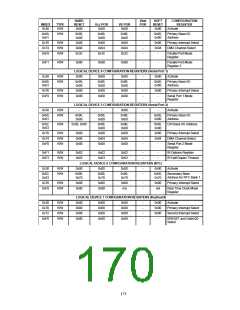
Chip (Global) Control Registers
0x00 -
0x01
Reserved - Writes are ignored, reads return 0.
Config Control
0x02 W
The hardware automatically clears this bit after the
write, there is no need for software to clear the bits.
Bit 0 = 1: Soft Reset. Refer to the "Configuration
Registers" table for the soft reset value for each
register.
C
Default = 0x00
on Vcc POR or
Reset_Drv
Index Address
0x03 R/W
Bit[7]
= 1 Enable GP1, WDT_CTRL, GP5, GP6, Soft Power
Enable and Status Register access when not in
configuration mode
Default = 0x03
= 0 Disable GP1, WDT_CTRL, GP5, GP6, Soft Power
Enable and Status Register access when not in
configuration mode (Default)
on Vcc POR or
Reset_Drv
Bits [6:2]
Reserved - Writes are ignored, reads return 0.
Bits[1:0]
Sets GP1 etc. selection register used when in Run
mode (not in Configuration Mode).
= 11 0xEA (Default)
= 10 0xE4
= 01 0xE2
= 00 0xE0
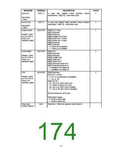
0x04 - 0x06 Reserved - Writes are ignored, reads return 0.
Logical Device #
Default = 0x00
on Vcc POR or
Reset_Drv
0x07 R/W
A write to this register selects the current logical
device. This allows access to the control and
configuration registers for each logical device. Note:
the Activate command operates only on the selected
logical device.
C
Card Level
Reserved
0x08 - 0x1F Reserved - Writes are ignored, reads return 0.
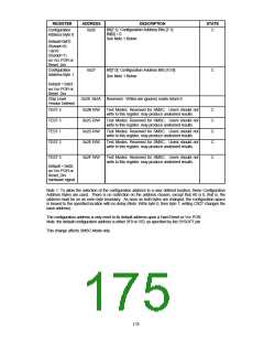
Chip Level, SMSC Defined
176

 SMSC [ SMSC CORPORATION ]