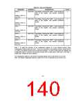
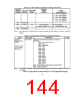
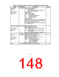
Table 56 - I/O Base Address Configuration Register Description
BASE I/O
LOGICAL
DEVICE LOGICAL REGISTER
NUMBER DEVICE INDEX
RANGE
(NOTE3)
FIXED
BASE OFFSETS
+3 : CIrCC SCE Registers
+4 : CIrCC SCE Registers
+5 : CIrCC SCE Registers
+6 : CIrCC SCE Registers
+7 : CIrCC SCE Registers
0x06
0x07
Reserved
KYBD
Not Relocatable
+0 : Data Register
n/a
Fixed Base Address: 60,64 +4 : Command/Status Reg.
0x09
Reserved
Note 3: This chip uses ISA address bits [A11:A0] to decode the base address of each of its logical
devices.
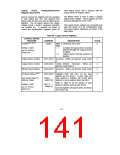
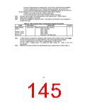
Table 57 - Interrupt Select Configuration Register Description
NAME
Interrupt
REG INDEX
DEFINITION
STATE
0x70 (R/W)
Bits[3:0] selects which interrupt level is used for
C
Request Level
Select 0
Interrupt 0.
0x00= no interrupt selected
0x01= IRQ1
0x02= IRQ2/nSMI
0x03= IRQ3
0x04= IRQ4
Default = 0x00
on Vcc POR or
Reset_Drv
0x05= IRQ5
0x06= IRQ6
0x07= IRQ7
0x08= IRQ8
0x09= IRQ9
0x0A= IRQ10
0x0B= IRQ11
0x0C= IRQ12
0x0D= IRQ13
0x0E= IRQ14
0x0F= IRQ15
Note: All interrupts are edge high (except ECP/EPP)
Note: nSMI is active low
Note:
An Interrupt is activated by setting the Interrupt Request Level Select 0 register to a non-zero
value AND :
For the FDC logical device by setting DMAEN, bit D3 of the Digital Output Register.
144

 SMSC [ SMSC CORPORATION ]