SYSTEM MANAGEMENT INTERRUPT (SMI)
The FDC37B77x implements a group nSMI
This register is used to enable additional
interrupt sources onto the group nSMI output.
output pin. The System Management Interrupt
is a non-maskable interrupt with the highest
priority level used for transparent power
management. The nSMI group interrupt output
consists of the enabled interrupts from each of
the functional blocks in the chip. The interrupts
are enabled onto the group nSMI output via the
SMI Enable Registers 1 and 2. The nSMI output
is then enabled onto the group nSMI output pin
via bit[7] in the SMI Enable Register 2.
This register is also used to enable the group
nSMI output onto the nSMI Serial/Parallel IRQ
pin and the routing of 8042 P12 internally to
nSMI.
SMI Status Registers
SMI Status Register 1
(Configuration Register B6, Logical Device 8)
This register is used to read the status of the
SMI input events. Note: The status bit gets set
whether or not the interrupt is enabled onto the
group SMI output.
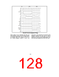
The logic equation for the nSMI output is as
follows:
nSMI
=
(EN_PINT and IRQ_PINT) or
(EN_U2INT and IRQ_U2INT) or
(EN_U1INT and IRQ_U1INT) or
(EN_FINT
(EN_WDT
(EN_MINT
(EN_KINT
and
and
and
and
IRQ_FINT)
IRQ_WDT)
IRQ_MINT)
IRQ_KINT)
or
or
or
or
SMI Status Register 2
(Configuration Register B7, Logical Device 8)
PME SUPPORT
(EN_IRINT and IRQ_IRINT)
The FDC37B77x offers support for PCI power
REGISTERS
management events (PMEs).
A
power
management event is requested by a PCI
function via the assertion of the nPME signal.
The assertion and deassertion of nPME is
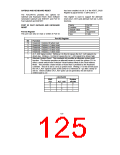
The following registers can be accessed when in
configuration mode at Logical Device 8,
Registers B4-B7 and when not in configuration
they can be accessed through the Index and
Data Register (refer to Table 49B).
asynchronous to the PCI clock.
In the
FDC37B77x, only active transitions on the ring
indicator inputs nRI1 and nRI2, valid NEC
infrared remote control frames, active keyboard-
clock edges and active mouse-clock edges can
assert the nPME signal. Note: The keyboard-
data and mouse-data pins are inactive (tri-state)
when VCC = 0V and VTR = 5V
SMI Enable Registers
SMI Enable Register 1
(Configuration Register B4, Logical Device 8)
This register is used to enable the different
interrupt sources onto the group nSMI output.
nPME functionality is controlled by the
configuration registers in logical device number
SMI Enable Register 2
eight.
The PME Enable bit, PME_En,
(Configuration Register B5, Logical Device 8)
LD8:CRC5.0, globally controls PME Wake-up
events. When PME_En is inactive, the nPME
signal can not be asserted. When PME_En is
asserted, any wake source whose individual
129

 SMSC [ SMSC CORPORATION ]