cleared.
There is no output pin
Status Register
associated with this internal signal.
This register is cleared on a reset. This register
is read-only for the Host and read/write by the
FDC37B77x CPU.
OBF
(Output Buffer Full) - This flag is set to
whenever the FDC37B77x CPU write to
the output data register (DBB). When
the host system reads the output data
register, this bit is automatically reset.
UD
Writable by FDC37B77x CPU. These
bits are user-definable.
C/D
(Command Data)-This bit specifies
whether the input data register contains
data or a command (0 = data, 1 =
EXTERNAL CLOCK SIGNAL
The FDC37B77x Keyboard Controller clock
source is a 12 MHz clock generated from a
14.318 MHz clock. The reset pulse must last for
at least 24 16 MHz clock periods. The pulse-
width requirement applies to both internally (Vcc
POR) and externally generated reset signals. In
powerdown mode, the external clock signal is
not loaded by the chip.
command).
During
a
host
data/command write operation, this bit
is set to "1" if SA2 = 1 or reset to "0" if
SA2 = 0.
IBF
(Input Buffer Full)- This flag is set to 1
whenever the host system writes data
into the input data register. Setting this
flag activates the FDC37B77x CPU's
nIBF (MIRQ) interrupt if enabled. When
the FDC37B77x CPU reads the input
data register (DBB), this bit is
automatically reset and the interrupt is
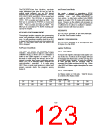
DEFAULT RESET CONDITIONS
The FDC37B77x has one source of reset: an
external reset via the RESET_DRV pin. Refer to
Table 51 for the effect of each type of reset on
the internal registers.
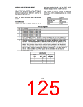
Table 51 - Resets
DESCRIPTION
KCLK
HARDWARE RESET (RESET)
Input
Input
Input
Input
N/A
KDAT
MCLK
MDAT
Host I/F Data Reg
Host I/F Status Reg
00H
N/A: Not Applicable
124

 SMSC [ SMSC CORPORATION ]