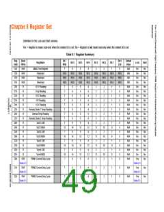
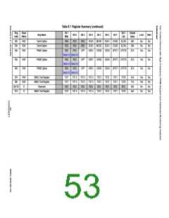
Chapter 8 Register Set
Definition for the Lock and Start columns:
Yes = Register is made read-only when the related bit is set; No = Register is not made read-only when the related bit is set.
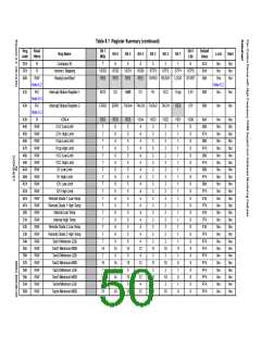
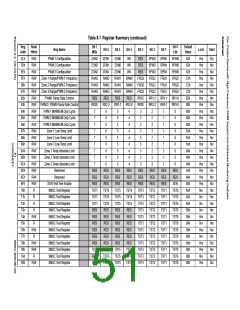
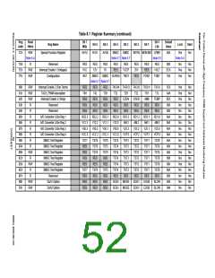
Table 8.1 Register Summary
Reg
Read
Bit 7
MSb
Bit 0
LSb
Default
Value
Reg Name
Bit 6
Bit 5
Bit 4
Bit 3
Bit 2
Bit 1
Lock
Start
Addr
/Write
10h
1Dh
1Eh
1Fh
20h
21h
22h
23h
24h
25h
26h
27h
28h
29h
2Ah
2Bh
2Ch
2Dh
2Eh
2Fh
30h
R/W
R/W
R/W
R/W
R
R
R
R
R
R
R
R
R
R
R
R
R
SMSC Test Register
Reserved
7
RES
RES
RES
7
7
7
7
7
7
7
7
7
15
7
15
7
15
7
15
7
6
RES
RES
RES
6
6
6
6
6
6
6
6
6
14
6
14
6
14
6
14
6
5
RES
RES
RES
5
5
5
5
5
5
5
5
5
13
5
13
5
13
5
13
5
4
RES
RES
RES
4
4
4
4
4
4
4
4
4
12
4
12
4
12
4
12
4
3
RES
RES
RES
3
3
3
3
3
3
3
3
3
11
3
11
3
11
3
11
3
2
RES
RES
RES
2
2
2
2
2
2
2
2
2
10
2
10
2
10
2
10
2
1
RES
RES
RES
1
1
1
1
1
1
1
1
1
9
1
9
1
0
RES
RES
RES
0
0
0
0
0
0
0
0
0
8
0
8
0
00h
00h
00h
00h
N/A
N/A
N/A
N/A
N/A
N/A
N/A
N/A
N/A
N/A
N/A
N/A
N/A
N/A
N/A
N/A
N/A
No
No
No
No
No
No
No
No
No
No
No
No
No
No
No
No
No
No
No
No
No
No
No
No
No
No
No
No
No
No
No
No
No
No
No
No
No
No
Reserved
Reserved
+2.5V Reading
Vccp Reading
VCC Reading
+5V Reading
+12V Reading
Remote Diode 1 Temp Reading
Internal Temp Reading
Remote Diode 2 Temp Reading
Tach1 LSB
Tach1 MSB
Tach2 LSB
Tach2 MSB
Tach3 LSB
Tach3 MSB
Tach4 LSB
Tach4 MSB
R
R
R
9
1
9
1
8
0
8
0
No
No
No
R/W
Note 8.1
R/W
Note 8.1
R/W
Note 8.1
PWM1 Current Duty Cycle
Yes
Note 8.1
Yes
Note 8.1
Yes
Note 8.1
31h
32h
PWM2 Current Duty Cycle
PWM3 Current Duty Cycle
7
7
6
6
5
5
4
4
3
3
2
2
1
1
0
0
N/A
N/A
No
No

 SMSC [ SMSC CORPORATION ]