Fan Control Device with Hardware Monitoring and Acoustic Noise Reduction Features
Datasheet
Chapter 9 Timing Diagrams
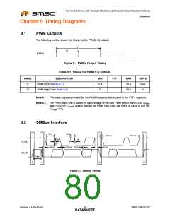
9.1
PWM Outputs
The following section shows the timing for the PWM[1:3] outputs.
t1
t2
FANx
Figure 9.1 PWMx Output Timing
Table 9.1 Timing for PWM[1:3] Outputs
NAME
DESCRIPTION
PWM Period (Note 9.1)
PWM High Time (Note 9.2)
MIN
TYP
MAX
UNITS
t1
t2
11.4
0
90.9
99.6
msec
%
Note 9.1 This value is programmable by the PWM frequency bits located in the FRFx registers.
Note 9.2 The PWM High Time is based on a percentage of the total PWM period (min=0/256*TPWM
,
max =255/256*TPWM). During Spin-up the PWM High Time can reach a 100% or Full On.
(TPWM = t1).
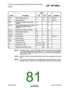
9.2
SMBus Interface
tLOW
tHIGH
tHD:STA
tSU:STO
tR
tF
SCLK
SDAT
tHD:STA
tHD:DAT tSU:DAT
tSU:STA
tBUF
P
S
S
P
Figure 9.2 SMBus Timing
Revision 0.4 (04-05-05)
SMSC EMC6D102
DATA8S0HEET

 SMSC [ SMSC CORPORATION ]