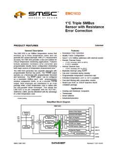
1°C Triple SMBus Sensor with Resistance Error Correction
Datasheet
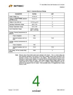
Table 1.3 Absolute Maximum Ratings
PARAMETER
Supply Voltage VDD
RATING
UNIT
-0.3 to 5.0
-0.3 to 5.5
V
V
Voltage on ALERT/THERM2, SMDATA
and SMCLK pins
Voltage on any other pin
-0.3 to VDD+0.3
-40 to +125
V
Operating Temperature Range
Storage Temperature Range
Lead Temperature Range
°C
°C
-55 to +150
Refer to JEDEC
Spec. J-STD-020
Package Thermal Characteristics for
MSOP-8
Power Dissipation
TBD
Thermal Resistance (at 0 air
flow)
109.6
°C/W
Package Thermal Characteristics for
SOIC-8
Power Dissipation
TBD
Thermal Resistance (at 0 air
flow)
135.9
°C/W
ESD Rating, All Pins (Human Body
Model)
2000
V
Note: Stresses above those listed could cause damage to the device. This is a stress rating only
and functional operation of the device at any other condition above those indicated in the
operation sections of this specification is not implied. When powering this device from
laboratory or system power supplies, it is important that the Absolute Maximum Ratings not be
exceeded or device failure can result. Some power supplies exhibit voltage spikes on their
outputs when the AC power is switched on or off. In addition, voltage transients on the AC
power line may appear on the DC output. If this possibility exists, it is suggested that a clamp
circuit be used.
Revision 1.1 (01-19-07)
4
SMSC EMC1033
DATASHEET

 SMSC [ SMSC CORPORATION ]