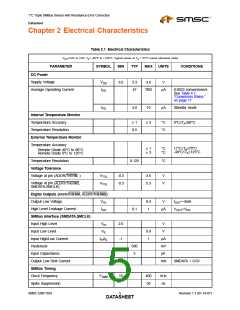
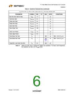
1°C Triple SMBus Sensor with Resistance Error Correction
Datasheet
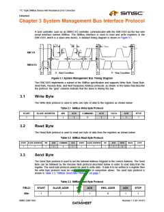
Chapter 1 Pin Configuration
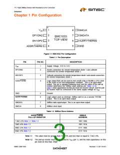
VDD
DP1/DN2
1
2
3
4
8
7
6
5
SMCLK
SMDATA
ALERT/THERM2
GND
EMC1033
TOP VIEW
DN1/DP2
ADDR/THERM
Figure 1.1 EMC1033 Pin Configuration
Table 1.1 Pin Description
PIN
PIN NO.
DESCRIPTION
Supply Voltage, 3.0V to 3.6V.
VDD
1
2
DP1/DN2
Anode connection for remote temperature diode 1 and cathode
connection for remote temperature diode 2.
DN1/DP2
3
4
Cathode connection for remote temperature diode1 and anode connection
for remote temperature diode 2.
ADDR/THERM
Logic output that can be used to turn on/off a fan or throttle a CPU clock
in the event of an over-temperature condition. This is an open-drain
output. This pin is sampled following reset and the value of the pull up
resistor determines the SMBus slave address per Table 1.2 on
page 3.Total capacitance on this pin must not exceed 100 pF, and the pull-
up resistor must be connected to the same supply voltage as VDD
Ground.
.
GND
5
ALERT/THERM2
6
Logic output used as interrupt, SMBus alert or as a second THERM
output. This is an open-drain output.
SMDATA
SMCLK
7
8
SMBus data input/output. This is an open-drain output.
SMBus clock input.
Table 1.2 SMBus Slave Address
ADDR/THERM
PULL-UP RESISTOR
SMBUS
ADDRESS
7.5kΩ ±5% Note 1.1, Note 1.2
12kΩ ±5% Note 1.2
1001 100b
1001 101b
0111 100b
0111 101b
20kΩ ±5% Note 1.2
33kΩ ±5% Note 1.2
Note 1.1 This value must be greater than 1kΩ ±5% and less than or equal to 7.5kΩ ±5%.
Note 1.2 The pull-up resistor must be connected to VDD (pin 1), and the total capacitance on this
pin must be less than 100pF.
SMSC EMC1033
3
Revision 1.1 (01-19-07)
DATASHEET

 SMSC [ SMSC CORPORATION ]