5Mbps ARCNET (ANSI 878.1) Controller with 2K x 8 On-Chip RAM
Datasheet
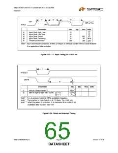
t1
t3
t2
4.0V
50% of VDD
1.0V
XTAL1
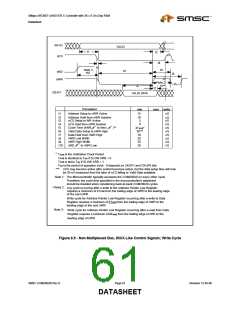
Parameter
min
typ
max units
nS
nS
nS
t1
t2
t3
t4
t5
Input Clock High Time
Input Clock Low Time
Input Clock Period
Input Clock Frequency
Frequency Accuracy*
10
10
25
10
-200
100
40
200
MHz
ppm
+
Note*: Input clock frequency must be 20 MHz ( 100ppm or better) to use the internal Clock Multiplier.
-
t is applied to crystal oscillaton.
5
Figure 8.13 - TTL Input Timing on XTAL1 Pin
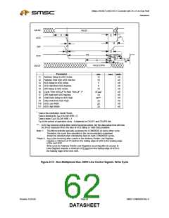
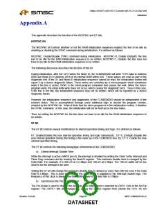
t1
nRESET
nINTR
t2
Parameter
min
typ
max units
*
t1
t2
nRESET Pulse Width***
nINTR High to Next nINTR Low
5TXTL
EF = 0
EF = 1
TDR**/2
4TXTL
*
Note*: TXTL is period of external XTAL oscillation frequency.
Note**: TDR is period of Data Rate (i.e. at 2.5 Mbps, TDR = 400 nS)
Note***: When the power is turned on, t1 is measured from stable XTAL
oscillation after VDD was over 4.5V.
Figure 8.14 - Reset and Interrupt Timing
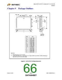
SMSC COM20020I Rev D
Page 65
Revision 12-05-06
DATASHEET

 SMSC [ SMSC CORPORATION ]