ST7781
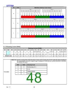
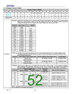
11.1.9 Display Control 3 (R09h)
Display Control 3 (R09h)
RS
/WR
/RD
D15 D14 D13 D12 D11 D10
D9
PTS
1
D8
PTS
0
D7
0
D6
0
D5
D4
D3
ICS
3
D2
ICS
2
D1
ICS
1
D0
ICS
0
PTS
PTG PTG
0
0
0
0
0
0
0
0
0
0
1
↑
1
2
0
1
0
0
0
0
0
0
0
0
0
0
0
Default value
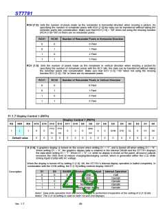
ICS [3:0]: Set the scan cycle when PTG [1:0] selects interval scan in non-display area drive period. The scan cycle is
defined by n frame periods, where n is an odd number from 0 to 29. The polarity of liquid crystal drive
voltage from the gate driver is inverted in the same timing as the interval scan cycle.
ICS[3:0]
Scan Cycle
fFLM = 60Hz
-
0000
0001
0010
0011
0100
0101
0110
0111
1000
1001
1010
1011
1100
1101
1110
1111
0 frame
1 frame
17ms
3 frame
50ms
5 frame
84ms
7 frame
117ms
150ms
184ms
217ms
251ms
284ms
317ms
351ms
384ms
418ms
451ms
484ms
9 frame
11 frame
13 frame
15 frame
17 frame
19 frame
21 frame
23 frame
25 frame
27 frame
29 frame
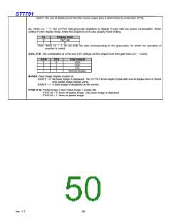
PTG [1:0]: Sets the scan mode in non-display area. The scan mode selected by PTG [1:0] bits is applied in the
non-display area when the base image is turned off and the non-display area other than the first and
second partial display areas.
Description
PTG[1:0]
Gate Output in Non-Display Area
Normal Scan
Source Output in Non-Display Area
VCOM Output
00
01
10
11
Set with the PTS[2:0]
VCOMH/VCOML
Setting Prohibited
Interval Scan
-
-
Set with the PTS[2:0]
0
VCOMH/VCOML
-
Setting Prohibited
PTS [2:0]: Sets the source output level in non-display area drive period. When PTS[2] = 1, the operation of amplifiers
which generates the grayscales other than V0 and V63 are halted and the step-up clock frequency
becomes half the normal frequency in non-display drive period in order to reduce power consumption.
Grayscale
Amplifier
in Operation
Source Output Level
PTS[2:0]
Step-Up Clock Frequency
Positive Polarity
Negative Polarity
000
001
010
011
100
101
110
111
V63
Setting inhibited
GND
V0
Setting inhibited
GND
V63 to V0
-
Register Setting (DC1,DC0)
-
V63 to V0
V63 to V0
V63 and V0
-
Register Setting(DC1,DC0)
Register Setting(DC1,DC0)
Frequency setting by(DC1,DC0)
-
Hi-Z
Hi-Z
V63
V0
Setting inhibited
GND
Setting inhibited
GND
V63 and V0
V63 and V0
Frequency setting by(DC1,DC0)
Frequency setting by (DC1,DC0)
Hi-Z
Hi-Z
Note1: The power efficiency improved by halting grayscale amplifiers and slowing down the step-up clock frequency
can be obtained in non-display drive period.
Ver. 1.7
52

 SITRONIX [ SITRONIX TECHNOLOGY CO., LTD. ]