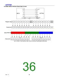
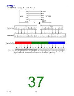
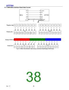
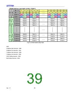
ST7781
10 Serial Peripheral Interfaces (SPI)
10.1 General Description
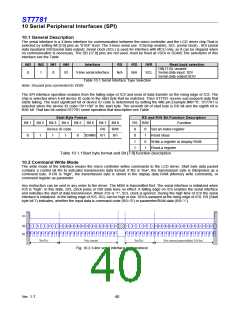
The serial interface is a 3-lines interface for communication between the micro controller and the LCD driver chip.That is
selected by setting IM [3:0] pins as “010X” level. The 3-lines serial use: /CS(chip enable), SCL (serial clock) , SDI (serial
data input)and SDO(serial data output). Serial clock (SCL) is used for interface with MCU only, so it can be stopped when
no communication is necessary. The DB [17:0] pins are not used, must be fixed at VDDI or DGND.The selections of this
interface see the Table
IM3
IM2
IM1
IM0
Interface
RS
/RD
/WR
Read back selection
DB[17:0]: unused
0
1
0
ID
3-line serial interface
N/A
N/A
SCL
Serial data input :SDI
Serial data output:SDO
Table 10.1 Serial Interface Type Selection
Note: Unused pins connected to VDDI.
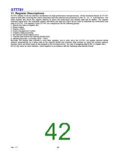
The SPI interface operation enables from the falling edge of /CS and ends of data transfer on the rising edge of /CS. The
chip is selected when 6-bit device ID code in the start byte that be matched. Then ST7781 receive sub-sequent data that
starts taking. The least significant bit of device ID code is determined by setting the IM0 pin.Example:IM0=”0”, ST7781 is
selected when the device ID code=”011100” in the start byte. The seventh bit of start byte is RS bit and the eighth bit is
R/W bit. That two bit control ST7781 some operation that description see Table
Start Byte Format
RS and R/W Bit Function Description
RS R/W Function
Set an index register
Bit 1 Bit 2 Bit 3 Bit 4 Bit 5 Bit 6 Bit 7 Bit 8
Device ID code
RS
R/W
0/1
0
0
1
1
0
1
0
1
0
1
1
1
0
ID/IM0 0/1
Read staus
Write a register or display RAM
Read a register
Table 10.1.1Start byte format and Bit [7:8] function description
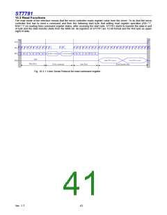
10.2 Command Write Mode
The write mode of the interface means the micro controller writes commands to the LCD driver. Start byte data packet
contains a control bit RS to indicates transmission data format. If RS is “low”, the transmission byte is interpreted as a
command byte. If RS is “high”, the transmission byte is stored in the display data RAM (Memory write command), or
command register as parameter.
Any instruction can be sent in any order to the driver. The MSB is transmitted first. The serial interface is initialized when
/CS is “high”. In this state, SCL clock pulse or SDI data have no effect. A falling edge on /CS enables the serial interface
and indicates the start of data transmission. When /CS is “1”, SCL clock is ignored. During the high time of /CS the serial
interface is initialized. At the falling edge of /CS, SCL can be high or low. SDI is sampled at the rising edge of /CS. RS (Start
byte bit 7) indicates, whether the input data is command code (RS=’0’) or parameter/RAM data (RS=’1’).
Fig. 10.2 3-line serial interface write protocol
Ver. 1.7
40

 SITRONIX [ SITRONIX TECHNOLOGY CO., LTD. ]