ST7781
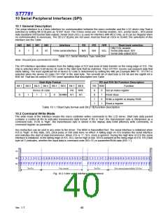
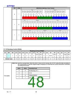
11.1.1 Index (IR)
Index(IR)
RS
/WR
/RD
D15 D14 D13 D12 D11 D10
D9
D8
D7
D6
D5
D4
D3
D2
D1
D0
-
-
-
-
-
-
-
-
ID7
ID6
ID5
ID4
ID3
ID2
ID1
ID0
0
↑
1
Note: “-“Don’t care
The index register specifies the index R00h to RFFh of the control register or RAM control to be accessed. The
access to the register and instruction bits in it is prohibited unless the index is specified in the index register.
Description
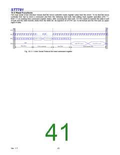
11.1.2 Device ID Code Read (R00h)
Device ID Code Read Out (R00h)
RS
/WR
/RD
D15 D14 D13 D12 D11 D10
D9
D8
D7
D6
D5
D4
D3
D2
D1
D0
0
1
1
1
0
1
1
1
1
0
0
0
0
0
1
1
1
1
↑
Description
When read this register, the device output device ID code
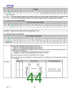
11.1.3 Device Output Control (R01H)
Device Output Control (R01H)
RS
/WR
/RD
D15 D14 D13 D12 D11 D10
D9
0
D8
SS
0
D7
0
D6
0
D5
0
D4
0
D3
0
D2
0
D1
0
D0
0
0
0
0
0
0
0
0
0
0
0
SM
0
1
↑
1
0
0
0
0
0
0
0
0
0
Default value
SS: Select the shift direction of outputs from the source driver.
When SS = 0, the shift direction of outputs is from S1 to S720
When SS = 1, the shift direction of outputs is from S720 to S1.
In addition to the shift direction, the settings for both SS and BGR bits are required to change the Assignment of R, G,
B dots to the source driver pins.
To assign R, G, B dots to the source driver pins from S1 to S720, set SS = 0.
To assign R, G, B dots to the source driver pins from S720 to S1, set SS = 1.
Note: When changing SS or BGR bits, DRAM data must be rewritten.
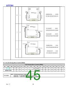
SM: Sets the gate driver pin arrangement in combination with the GS bit (R60h) to select the optimal scan mode for
the module.
SM
GS
Scan Direction
Gate Output Sequence
Description
G1,G2,G3,G4…..,G316
G317,G318,G319, G320
0
0
Ver. 1.7
44

 SITRONIX [ SITRONIX TECHNOLOGY CO., LTD. ]