ST7781
6. Pin Description
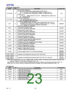
6.1 Power Supply Pin
Name
VDD
I/O
Description
Power supply for analog, digital system and booster circuit
Power supply for I/O system
Connect Pin
VDD
I
I
I
I
VDDI
VDDI
GND
GND
AGND
DGND
System ground for analog system and booster circuit.
System ground for I/O system and internal digital system.
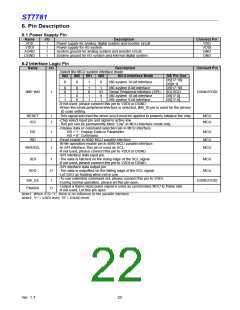
6.2 Interface Logic Pin
Name
I/O
Description
Connect Pin
-Select the MCU system interface mode
IM3
IM2
IM1
IM0
MCU-Interface Mode
DB Pin Use
DB[17:10]
DB[8:1]
0
0
1
0
I80-system 16-bit interface
0
0
1
1
0
1
0
0
1
0
1
1
1
ID
0
I80-system 8-bit interface
Serial Peripheral interface (SPI)
I80-system 18-bit interface
I80-system 9-bit interface
DB[17:10]
SDI,SDO
DB[17:0]
DB[17:9]
IM0~IM3
I
DGND/VDDI
1
-If not used, please connect this pin to VDDI or DGND
-When the serial peripheral interface is selected, IM0_ID pin is used for the device
ID code setting.
RESET
/CS
I
I
-This signal will reset the driver and it must be applied to properly initialize the chip.
MCU
MCU
-Chip select input pin and signal is active low.
-This pin can be permanently fixed “Low” in MCU interface mode only.
-Display data or command selection pin in MCU interface.
RS =’1’: Display Data or Parameter.
RS
/RD
I
I
I
MCU
MCU
MCU
RS =’0’: Command.
-Read enable in 8080 MCU parallel interface.
-Write operation enable pin in 8080 MCU parallel interface.
-In SPI interface, this pin is used as SCL.
/WR/SCL
-If not used, please connect this pin to VDDI or DGND.
-SPI interface data input pin.
SDI
I
-The data is latched on the rising edge of the SCL signal.
-If not used, please connect this pin to VDDI or DGND.
-SPI interface data output pin.
-The data is outputted on the falling edge of the SCL signal.
-Let SDO as floating when not in use.
MCU
MCU
SDO
O
-To use extended command set, please connect this pin to VDDI.
-During normal operation, please let this pin open.
-Output a frame head pulse signal is used as synchronies MCU to frame rate
-If not used, Let this pin open
SW_EE
FMARK
I
DGND/VDDI
-
O
Note1. When /CS=”1”, there is no influence to the parallel interface.
Note2. “1” = VDDI level, “0” = DGND level.
Ver. 1.7
22

 SITRONIX [ SITRONIX TECHNOLOGY CO., LTD. ]