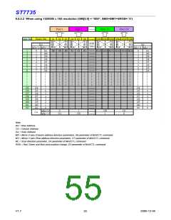
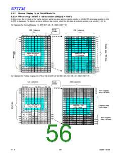
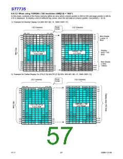
ST7735
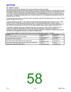
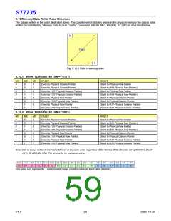
9.10 Memory Data Write/ Read Direction
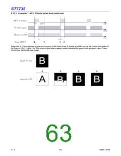
The data is written in the order illustrated above. The Counter which dictates where in the physical memory the data is to be
written is controlled by “Memory Data Access Control” Command, bits B5 (MV), B6 (MX), B7 (MY) as described below.
Panel
Fig. 9.10.1 Data streaming order
9.10.1 When 128RGBx160 (GM= “011”)
MV
0
MX
0
MY
0
CASET
RASET
Direct to Physical Column Pointer
Direct to Physical Column Pointer
Direct to (127-Physical Column Pointer)
Direct to (127-Physical Column Pointer)
Direct to Physical Row Pointer
Direct to (159-Physical Row Pointer)
Direct to Physical Row Pointer
Direct to (159-Physical Row Pointer)
Direct to Physical Row Pointer
Direct to (159-Physical Row Pointer)
Direct to Physical Row Pointer
Direct to (159-Physical Row Pointer)
Direct to Physical Column Pointer
Direct to Physical Column Pointer
Direct to (127-Physical Column Pointer)
Direct to (127-Physical Column Pointer)
0
0
1
0
1
0
0
1
1
1
0
0
1
0
1
1
1
0
1
1
1
9.10.2 When 132RGBx162 (GM= “000”)
MV
0
MX
0
MY
0
CASET
RASET
Direct to Physical Column Pointer
Direct to Physical Column Pointer
Direct to (131-Physical Column Pointer)
Direct to (131-Physical Column Pointer)
Direct to Physical Row Pointer
Direct to (161-Physical Row Pointer)
Direct to Physical Row Pointer
Direct to (161-Physical Row Pointer)
Direct to Physical Row Pointer
Direct to (161-Physical Row Pointer)
Direct to Physical Row Pointer
Direct to (161-Physical Row Pointer)
Direct to Physical Column Pointer
Direct to Physical Column Pointer
Direct to (131-Physical Column Pointer)
Direct to (131-Physical Column Pointer)
0
0
1
0
1
0
0
1
1
1
0
0
1
0
1
1
1
0
1
1
1
Note: Data is always written to the Frame Memory in the same order, regardless of the Memory Write Direction set by MADCTL bits B7
(MY), B6 (MX), B5 (MV). The write order for each pixel unit is
One pixel unit represents 1 column and 1page counter value on the Frame Memory.
V1.7
59
2009-12-04

 SITRONIX [ SITRONIX TECHNOLOGY CO., LTD. ]