ABSOLUTE MAXIMUM RATINGS
These are stress ratings only and functional operation
of the device at these ratings or any other above those
indicated in the operation sections of the specifications
below is not implied. Exposure to absolute maximum
rating conditions for extended periods of time may
affect reliability and cause permanent damage to the
device.
Short-Circuit Duration
TxOUT .................................................... Continuous
Storage Temperature ...................... -65°C to +150°C
Power Dissipation per package
28-pin PDIP
(derate 16.0mW/°C above+70°C) ...................... 1300mW
20-pin SSOP
VCC ...................................................... -0.3V to +6.0V
V+ (NOTE 1) ...................................... -0.3V to +7.0V
V- (NOTE 1) ....................................... +0.3V to -7.0V
V+ + |V-| (NOTE 1)........................................... +13V
(derate 9.25mW/°C above +70°C) ...................... 750mW
20-pin TSSOP
(derate 11.1mW/°C above +70°C) ....................... 900mW
28-pin SOIC
I
(DC VCC or GND current)......................... +100mA
(derate 12.7mW/°C above +70°C) .................... 1000mW
28-pin SSOP
(derate 11.2mW/°C above +70°C) ...................... 900mW
28-pin TSSOP
(derate 11.1mW/°C above +70°C) ....................... 900mW
32-pin QFN
InCCput Voltages
TxIN, ONLINE,
SHUTDOWN, EN (SP3223E) ............ -0.3V to +6.0V
RxIN .................................................................. +25V
Output Voltages
TxOUT ........................................................... +13.2V
RxOUT, STATUS ..................... -0.3V to (VCC + 0.3V)
NOTE 1: V+ and V- can have maximum magnitudes of 7V, but their absolute difference cannot exceed 13V.
ELECTRICAL CHARACTERISTICS
Unless otherwise noted, the following specifications apply for VCC = +3.0V to +5.5V with TAMB = TMIN to TMAX
,
C1 - 4 = 0.1µF. Typical values apply at VCC = +3.3V or +5.0V and TAMB = 25°C.
PARAMETER
MIN.
TYP.
MAX. UNITS CONDITIONS
DC CHARACTERISTICS
Supply Current,
AUTO ON-LINE
1.0
10
10
µA
µA
All RxIN open, ONLINE = GND,
SHUTDOWN = VCC, TxIN = VCC or
GND,VCC = +3.3V, TAMB = +25°C
®
Supply Current, Shutdown
1.0
0.3
SHUTDOWN = GND,
VCC = +3.3V, TAMB = +25°C,
TxIN = VCC or GND
Supply Current,
AUTO ON-LINE Disabled
1.0
mA ONLINE = SHUTDOWN = VCC
TxIN = VCC or GND,
,
®
no load, VCC = +3.3V, TAMB = +25°C
LOGIC INPUTS AND RECEIVER OUTPUTS
Input Logic Threshold
VCC = +3.3V or +5.0V, TxIN,
EN (SP3223EB), ONLINE,
SHUTDOWN
LOW
HIGH
GND
2.4
0.8
VCC
V
V
Input Leakage Current
SHUTDOWN,
±0.01
±0.05
±1.0
µA
TxIN, EN (SP3223EB), ONLINE,
TAMB = +25°C, VIN = 0V to VCC
Output Leakage Current
±10
µA
Receivers disabled, VOUT = 0V to
VCC
Output Voltage LOW
Output Voltage HIGH
DRIVER OUTPUTS
Output Voltage Swing
0.4
V
V
IOUT = 1.6mA
IOUT = -1.0mA
VCC - 0.6 VCC - 0.1
±5.0
±5.4
±35
V
All driver outputs loaded with 3KΩ
to GND, TAMB = +25°C
Output Resistance
300
Ω
VCC = V+ = V- = 0V, VOUT = ±2V
Output Short-Circuit Current
Output Leakage Current
±60
±25
mA VOUT = 0V
µA VCC = 0V or 3.0V to 5.5V,
VOUT = ±12V, Drivers disabled
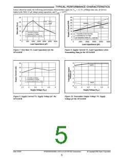
Date: 6/2/04
SP3223EB/3243EB +3.0V to +5.5V RS-232 Transceivers
© Copyright 2004 Sipex Corporation
2

 SIPEX [ SIPEX CORPORATION ]