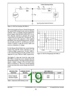
CCoonnttaacctt--DDiisscchhaarrggee MMoodduullee
R
R
R
R
S
S
R
R
V
V
C
C
SW2
SW2
SW1
SW1
Device
Under
Test
DC Power
Source
C
C
S
S
R
R
and R add up to 330Ω for IEC1000-4-2.
and R add up to 330Ω for IEC1000-4-2.
S
S
V
V
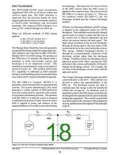
Figure 31. ESD Test Circuit for IEC1000-4-2
The circuit model in Figures 29 and 30 represent
the typical ESD testing circuit used for all three
methods. TheCS isinitiallychargedwiththeDC
power supply when the first switch (SW1) is on.
Now that the capacitor is charged, the second
switch(SW2)isonwhileSW1switchesoff. The
voltage stored in the capacitor is then applied
throughRS, thecurrentlimitingresistor, ontothe
device under test (DUT). In ESD tests, the SW2
switch is pulsed so that the device under test
receives a duration of voltage.
30A
15A
0A
FortheHumanBodyModel, thecurrentlimiting
resistor (RS) and the source capacitor (CS) are
1.5kΩ an 100pF, respectively. For IEC-1000-4-
2,thecurrentlimitingresistor(RS)andthesource
capacitor (CS) are 330Ω an 150pF, respectively.
t=0ns
t=30ns
t ➙
Figure 32. ESD Test Waveform for IEC1000-4-2
The higher CS value and lower RS value in the
IEC1000-4-2 model are more stringent than the
HumanBodyModel. Thelargerstoragecapacitor
injects a higher voltage to the test point when
SW2 is switched on. The lower current limiting
resistor increases the current charge onto the test
point.
DEVICE PIN
TESTED
HUMAN BODY
MODEL
IEC1000-4-2
Air Discharge Direct Contact
Level
Driver Outputs
Receiver Inputs
±15kV
±15kV
±15kV
±15kV
±8kV
±8kV
4
4
Table 4. Transceiver ESD Tolerance Levels
Date: 6/2/04
SP3223EB/3243EB +3.0V to +5.5V RS-232 Transceivers
© Copyright 2004 Sipex Corporation
19

 SIPEX [ SIPEX CORPORATION ]