Si4730/31/34/35-D60
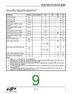
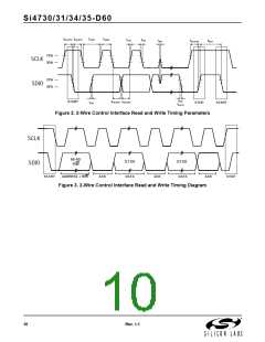
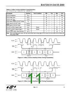
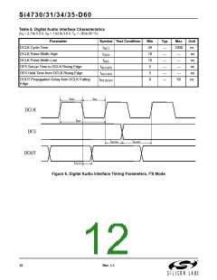
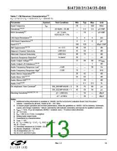
Table 4. 2-Wire Control Interface Characteristics1,2,3
(VA = 2.7 to 5.5 V, VD = 1.62 to 3.6 V, TA = –20 to 85 °C)
Parameter
Symbol Test Condition
Min
0
Typ
—
Max
400
—
Unit
kHz
µs
SCLK Frequency
SCLK Low Time
SCLK High Time
f
SCL
t
1.3
0.6
0.6
—
LOW
t
—
—
µs
HIGH
SCLK Input to SDIO Setup
t
t
—
—
µs
SU:STA
(START)
SCLK Input to SDIO Hold
0.6
—
—
µs
HD:STA
(START)
SDIO Input to SCLK Setup
t
t
100
0
—
—
—
—
900
—
ns
ns
µs
SU:DAT
4,5
SDIO Input to SCLK Hold
HD:DAT
SU:STO
SCLK input to SDIO Setup
t
0.6
(STOP)
STOP to START Time
SDIO Output Fall Time
t
1.3
—
—
—
µs
ns
BUF
t
250
f:OUT
Cb
----------
1pF
20 + 0.1
SDIO Input, SCLK Rise/Fall Time
t
t
—
300
ns
f:IN
r:IN
Cb
----------
1pF
20 + 0.1
SCLK, SDIO Capacitive Loading
Input Filter Pulse Suppression
Notes:
C
—
—
—
—
50
50
pF
ns
b
t
SP
1. When VD = 0 V, SCLK and SDIO are low impedance.
2. When selecting 2-wire mode, the user must ensure that a 2-wire start condition (falling edge of SDIO while SCLK is
high) does not occur within 300 ns before the rising edge of RST.
3. When selecting 2-wire mode, the user must ensure that SCLK is high during the rising edge of RST, and stays high
until after the first start condition.
4. The Si473x-D60 delays SDIO by a minimum of 300 ns from the VIH threshold of SCLK to comply with the minimum
tHD:DAT specification.
5. The maximum tHD:DAT has only to be met when fSCL = 400 kHz. At frequencies below 400 KHz, tHD:DAT may be
violated as long as all other timing parameters are met.
Rev. 1.1
9

 SILICON [ SILICON ]