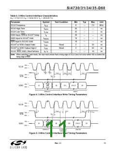
Si4730/31/34/35-D60
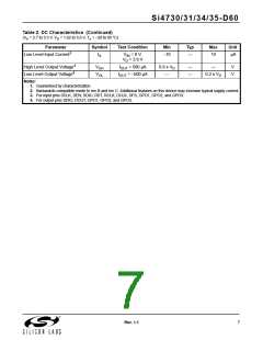
Table 2. DC Characteristics (Continued)
(VA = 2.7 to 5.5 V, VD = 1.62 to 3.6 V, TA = –20 to 85 °C)
Parameter
Symbol
Test Condition
= 0 V,
Min
Typ
Max
Unit
3
Low Level Input Current
I
V
–10
—
10
µA
IL
IN
V = 3.6 V
D
4
High Level Output Voltage
V
I
= 500 µA
0.8 x V
—
—
—
—
V
V
OH
OUT
D
4
Low Level Output Voltage
V
I
= –500 µA
0.2 x V
D
OL
OUT
Notes:
1. Guaranteed by characterization.
2. Backwards compatible mode to rev B and rev C. Additional features on this device may increase typical supply current.
3. For input pins SCLK, SEN, SDIO, RST, RCLK, DCLK, DFS, GPO1, GPO2, and GPO3.
4. For output pins SDIO, DOUT, GPO1, GPO2, and GPO3.
Rev. 1.1
7

 SILICON [ SILICON ]