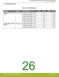
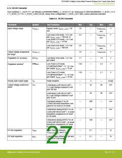
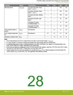
EFR32MG13 Mighty Gecko Multi-Protocol Wireless SoC Family Data Sheet
Electrical Specifications
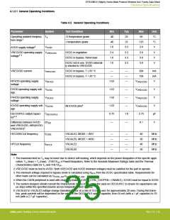
4.1.2.1 General Operating Conditions
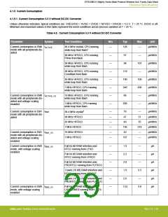
Table 4.2. General Operating Conditions
Parameter
Symbol
Test Condition
Min
-40
-40
1.8
Typ
25
Max
85
Unit
°C
°C
V
Operating ambient tempera- TA
ture range1
-G temperature grade
-I temperature grade
25
125
3.8
AVDD supply voltage2
VAVDD
3.3
VREGVDD operating supply VVREGVDD
voltage2 3
DCDC in regulation
2.4
1.8
1.8
3.3
3.3
3.3
3.8
3.8
3.8
V
V
V
DCDC in bypass, 50mA load
DCDC not in use. DVDD external-
ly shorted to VREGVDD
VREGVDD current
IVREGVDD
DCDC in bypass, T ≤ 85 °C
DCDC in bypass, T > 85 °C
—
—
—
—
—
200
100
mA
mA
V
RFVDD operating supply
voltage
VRFVDD
1.62
VVREGVDD
DVDD operating supply volt- VDVDD
age
1.62
1.62
1.62
0.75
—
—
VVREGVDD
VVREGVDD
VVREGVDD
2.75
V
V
PAVDD operating supply
voltage
VPAVDD
All IOVDD pins4
IOVDD operating supply volt- VIOVDD
age
—
V
DECOUPLE output capaci-
tor5 6
CDECOUPLE
1.0
µF
Difference between AVDD
dVDD
—
—
0.1
V
and VREGVDD, ABS(AVDD-
VREGVDD)2
HFCORECLK frequency
fCORE
VSCALE2, MODE = WS1
VSCALE0, MODE = WS0
VSCALE2
—
—
—
—
—
—
—
—
40
20
40
20
MHz
MHz
MHz
MHz
HFCLK frequency
fHFCLK
VSCALE0
Note:
1. The maximum limit on TA may be lower due to device self-heating, which depends on the power dissipation of the specific appli-
cation. TA (max) = TJ (max) - (THETAJA x PowerDissipation). Refer to the Absolute Maximum Ratings table and the Thermal
Characteristics table for TJ and THETAJA
.
2. VREGVDD must be tied to AVDD. Both VREGVDD and AVDD minimum voltages must be satisfied for the part to operate.
3. The minimum voltage required in bypass mode is calculated using RBYP from the DCDC specification table. Requirements for
other loads can be calculated as VDVDD_min+ILOAD * RBYP_max
.
4. When the CSEN peripheral is used with chopping enabled (CSEN_CTRL_CHOPEN = ENABLE), IOVDD must be equal to AVDD.
5. The system designer should consult the characteristic specs of the capacitor used on DECOUPLE to ensure its capacitance val-
ue stays within the specified bounds across temperature and DC bias.
6. VSCALE0 to VSCALE2 voltage change transitions occur at a rate of 10 mV / usec for approximately 20 usec. During this transi-
tion, peak currents will be dependent on the value of the DECOUPLE output capacitor, from 35 mA (with a 1 µF capacitor) to 70
mA (with a 2.7 µF capacitor).
silabs.com | Building a more connected world.
Rev. 1.4 | 25

 SILICON [ SILICON ]