EFR32MG13 Mighty Gecko Multi-Protocol Wireless SoC Family Data Sheet
Pin Definitions
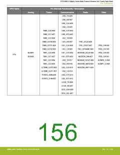
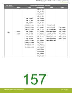
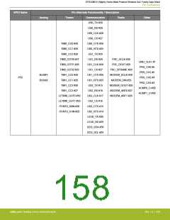
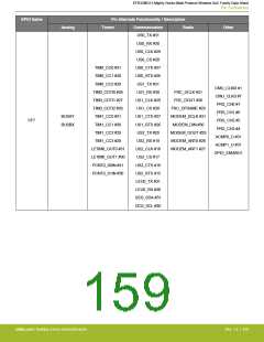
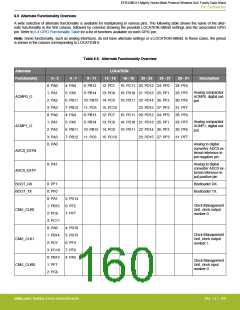
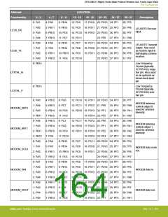
6.5 Alternate Functionality Overview
A wide selection of alternate functionality is available for multiplexing to various pins. The following table shows the name of the alter-
nate functionality in the first column, followed by columns showing the possible LOCATION bitfield settings and the associated GPIO
pin. Refer to 6.4 GPIO Functionality Table for a list of functions available on each GPIO pin.
Note: Some functionality, such as analog interfaces, do not have alternate settings or a LOCATION bitfield. In these cases, the pinout
is shown in the column corresponding to LOCATION 0.
Table 6.5. Alternate Functionality Overview
Alternate
LOCATION
12 - 15 16 - 19
Functionality
0 - 3
0: PA0
1: PA1
2: PA2
3: PA3
0: PA0
1: PA1
2: PA2
3: PA3
0: PA0
4 - 7
4: PA4
5: PA5
6: PB11
7: PB12
4: PA4
5: PA5
6: PB11
7: PB12
8 - 11
8: PB13
9: PB14
20 - 23
24 - 27
28 - 31
28: PF4
29: PF5
30: PF6
31: PF7
28: PF4
29: PF5
30: PF6
31: PF7
Description
12: PC7
13: PC8
16: PC11 20: PD12 24: PF0
18: PD10 21: PD13 25: PF1
19: PD11 22: PD14 26: PF2
23: PD15 27: PF3
Analog comparator
ACMP0, digital out-
put.
ACMP0_O
ACMP1_O
10: PB15 14: PC9
11: PC6
8: PB13
9: PB14
15: PC10
12: PC7
13: PC8
16: PC11 20: PD12 24: PF0
18: PD10 21: PD13 25: PF1
19: PD11 22: PD14 26: PF2
23: PD15 27: PF3
Analog comparator
ACMP1, digital out-
put.
10: PB15 14: PC9
11: PC6 15: PC10
Analog to digital
converter ADC0 ex-
ternal reference in-
put negative pin.
ADC0_EXTN
ADC0_EXTP
0: PA1
Analog to digital
converter ADC0 ex-
ternal reference in-
put positive pin.
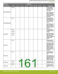
BOOT_RX
BOOT_TX
0: PF1
0: PF0
0: PA1
1: PB15
2: PC6
3: PC11
0: PA0
1: PB14
2: PC7
3: PC10
0: PB13
1: PF7
2: PC6
Bootloader RX.
Bootloader TX.
5: PD14
6: PF2
7: PF7
Clock Management
Unit, clock output
number 0.
CMU_CLK0
4: PD10
5: PD15
6: PF3
7: PF6
4: PA5
Clock Management
Unit, clock output
number 1.
CMU_CLK1
CMU_CLKI0
Clock Management
Unit, clock input
number 0.
silabs.com | Building a more connected world.
Rev. 1.4 | 160

 SILICON [ SILICON ]