C8051F39x/37x
With the CIP-51's maximum system clock at 48 MHz, it has a peak throughput of 48 MIPS. The CIP-51 has
a total of 109 instructions. The table below shows the total number of instructions that require each execu-
tion time.
Clocks to Execute
1
2
2/4
5
3
3/5
7
4
5
5
2
4/6
1
6
2
8
1
Number of Instructions
26
50
10
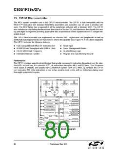
Programming and Debugging Support
In-system programming of the EPROM program memory and communication with on-chip debug support
logic is accomplished via the Silicon Labs 2-Wire Development Interface (C2).
The on-chip debug support logic facilitates full speed in-circuit debugging, allowing the setting of hardware
breakpoints, starting, stopping and single stepping through program execution (including interrupt service
routines), examination of the program's call stack, and reading/writing the contents of registers and mem-
ory. This method of on-chip debugging is completely non-intrusive, requiring no RAM, Stack, timers, or
other on-chip resources. C2 details can be found in Section “33. C2 Interface” on page 295.
The CIP-51 is supported by development tools from Silicon Labs and third party vendors. Silicon Labs pro-
vides an integrated development environment (IDE) including editor, debugger and programmer. The IDE's
debugger and programmer interface to the CIP-51 via the C2 interface to provide fast and efficient in-sys-
tem device programming and debugging. Third party macro assemblers and C compilers are also avail-
able.
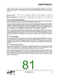
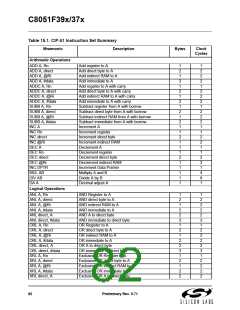
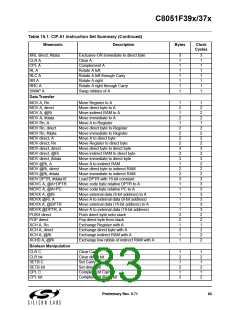
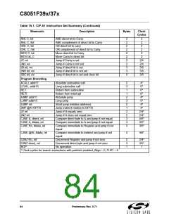
15.1. Instruction Set
The instruction set of the CIP-51 System Controller is fully compatible with the standard MCS-51™ instruc-
tion set. Standard 8051 development tools can be used to develop software for the CIP-51. All CIP-51
instructions are the binary and functional equivalent of their MCS-51™ counterparts, including opcodes,
addressing modes and effect on PSW flags. However, instruction timing is different than that of the stan-
dard 8051.
15.1.1. Instruction and CPU Timing
In many 8051 implementations, a distinction is made between machine cycles and clock cycles, with
machine cycles varying from 2 to 12 clock cycles in length. However, the CIP-51 implementation is based
solely on clock cycle timing. All instruction timings are specified in terms of clock cycles.
Due to the pipelined architecture of the CIP-51, most instructions execute in the same number of clock
cycles as there are program bytes in the instruction. Conditional branch instructions take one less clock
cycle to complete when the branch is not taken as opposed to when the branch is taken. Table 15.1 is the
CIP-51 Instruction Set Summary, which includes the mnemonic, number of bytes, and number of clock
cycles for each instruction.
Preliminary Rev. 0.71
81

 SILICON [ SILICON ]