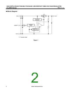
HIGH RIPPLE-REJECTION WLP PACKAGE LOW DROPOUT CMOS VOLTAGE REGULATOR
Rev.2.1_00
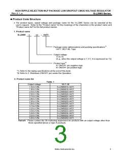
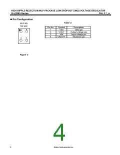
S-L2985 Series
Electrical Characteristics
Table 4
(Ta = 25°C unless otherwise specified)
Test
Circuit
Item
Symbol
VOUT(E)
Conditions
Min.
Typ.
Max.
Unit
VOUT(S) VOUT(S) VOUT(S)
Output voltage*1
VIN = VOUT(S) + 1.0 V, IOUT = 30 mA
VIN ≥ VOUT(S) + 1.0 V
V
1
× 0.99
150*5
⎯
⎯
⎯
× 1.01
⎯
Output current*2
Dropout voltage*3
IOUT
⎯
mA
V
3
1
Vdrop
IOUT = 100 mA
1.5 V ≤ VOUT(S) ≤ 1.6 V
0.32
0.28
0.25
0.20
0.19
0.55
0.47
0.35
0.29
0.26
1.7 V ≤ VOUT(S) ≤ 1.8 V
1.9 V ≤ VOUT(S) ≤ 2.3 V
2.4 V ≤ VOUT(S) ≤ 2.7 V
2.8 V ≤ VOUT(S) ≤ 5.5 V
⎯
⎯
ΔVOUT1
ΔVIN•VOUT
VOUT(S) + 0.5 V ≤ VIN ≤ 6.5 V,
IOUT = 30 mA
VIN = VOUT(S) + 1.0 V,
1.0 mA ≤ IOUT ≤ 80 mA
VIN = VOUT(S) + 1.0 V, IOUT = 10 mA,
−40°C ≤ Ta ≤ 85°C
Line regulation
Load regulation
⎯
⎯
⎯
⎯
0.05
12
0.2
40
⎯
% / V
mV
ΔVOUT2
ΔVOUT
ΔTa•VOUT
Output voltage
ppm
/ °C
±100
50
temperature coefficient*4
Current consumption
during operation
Current consumption
during shutdown
Input voltage
VIN = VOUT(S) + 1.0 V, ON/OFF pin = ON,
no load
ISS1
90
μA
2
VIN = VOUT(S) + 1.0 V, ON/OFF pin = OFF,
no load
ISS2
VIN
⎯
0.1
⎯
1.0
6.5
⎯
⎯
2.0
1.5
V
⎯
Shutdown pin
input voltage “H”
Shutdown pin
input voltage “L”
Shutdown pin
input current “H”
Shutdown pin
VSH
VIN = VOUT(S) + 1.0 V, RL = 1.0 kΩ
VIN = VOUT(S) + 1.0 V, RL = 1.0 kΩ
VIN = 6.5 V, VON/OFF = 6.5 V
VIN = 6.5 V, VON/OFF = 0 V
⎯
4
VSL
ISH
⎯
−0.1
−0.1
⎯
⎯
⎯
0.3
0.1
0.1
⎯
μA
ISL
⎯
input current “L”
VIN = VOUT(S) + 1.0 V, f = 1.0 kHz,
ΔVrip = 0.5 Vrms, IOUT = 30 mA
VIN = VOUT(S) + 1.0 V, ON/OFF pin = ON,
VOUT = 0 V
RR
Ripple rejection
80
dB
5
3
Short-circuit current
Ishort
⎯
200
⎯
mA
*1. VOUT(S): Specified output voltage
VOUT(E): Actual output voltage at the fixed load
The output voltage when fixing IOUT(= 30 mA) and inputting VOUT(S) + 1.0 V
*2. The output current at which the output voltage becomes 95% of VOUT(E) after gradually increasing the output current.
*3. Vdrop = VIN1 − (VOUT3 × 0.98)
VOUT3 is the output voltage when VIN = VOUT(S) + 1.0 V and IOUT = 100 mA.
VIN1 is the input voltage at which the output voltage becomes 98% of VOUT3 after gradually decreasing the input voltage.
*4. The change in temperature [mV/°C] is calculated using the following equation.
ΔVOUT
ΔTa
ΔVOUT
ΔTa • VOUT
*2
*3
[
mV/°C
]
*1 = VOUT(S)
[
V
]
×
[
ppm/°C
]
÷1000
*1. The change in temperature of the output voltage
*2. Specified output voltage
*3. Output voltage temperature coefficient
*5. The output current can be at least this value.
Due to restrictions on the package power dissipation, this value may not be satisfied. Attention should be paid to the power
dissipation of the package when the output current is large.
6
Seiko Instruments Inc.

 SII [ SEIKO INSTRUMENTS INC ]