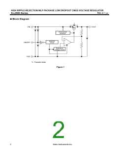
HIGH RIPPLE-REJECTION WLP PACKAGE LOW DROPOUT CMOS VOLTAGE REGULATOR
Rev.2.1_00
S-L2985 Series
Absolute Maximum Ratings
Table 3
(Ta = 25°C unless otherwise specified)
Item
Symbol
VIN
Absolute Maximum Rating
Unit
V
Input voltage
VSS − 0.3 to VSS + 7
VON/OFF
VOUT
PD
VSS − 0.3 to VIN + 0.3
VSS − 0.3 to VIN + 0.3
350*1
Output voltage
Power dissipation
mW
Operating ambient temperature
Storage ambient temperature
*1. When mounted on board
[Mounted board]
Topr
Tstg
−40 to +85
−40 to +125
°C
(1) Board size : 114.3 mm × 76.2 mm × t1.6 mm
(2) Board name : JEDEC STANDARD51-7
Caution The absolute maximum ratings are rated values exceeding which the product could suffer
physical damage. These values must therefore not be exceeded under any conditions.
600
500
400
300
200
100
0
0
50
100
150
Ambient Temperature Ta (°C)
Figure 3 Power Dissipation of Package (When Mounted on Board)
Seiko Instruments Inc.
5

 SII [ SEIKO INSTRUMENTS INC ]