STEP-DOWN, SYNCHRONOUS PWM CONTROL SWITCHING REGULATOR CONTROLLER
Rev.2.3_00
S-8533 Series
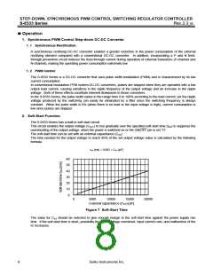
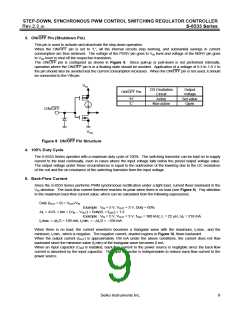
3. ON/OFF Pin (Shutdown Pin)
This pin is used to activate and deactivate the step-down operation.
When the ON/OFF pin is set to “L”, all the internal circuits stop working, and substantial savings in current
consumption are thus achieved. The voltage of the PDRV pin goes to VIN level and voltage of the NDRV pin goes
to VSS level to shut off the respective transistors.
The ON/OFF pin is configured as shown in Figure 8. Since pull-up or pull-down is not performed internally,
operation where the ON/OFF pin is in a floating state should be avoided. Application of a voltage of 0.3 to 1.8 V to
the pin should also be avoided lest the current consumption increases. When the ON/OFF pin is not used, it should
be connected to the VIN pin.
VIN
CR Oscillation
Circuit
Output
Voltage
ON/OFF Pin
“H”
“L”
Active
Set value
Open
Non-active
ON/OFF
VSS
Figure 8 ON/OFF Pin Structure
4. 100% Duty Cycle
The S-8533 Series operates with a maximum duty cycle of 100%. The switching transistor can be kept on to supply
current to the load continually, even in cases where the input voltage falls below the preset output voltage value.
The output voltage under these circumstances is equal to the subtraction of the lowering due to the DC resistance
of the coil and the on-resistance of the switching transistor from the input voltage.
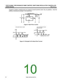
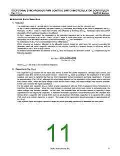
5. Back-Flow Current
Since the S-8533 Series performs PWM synchronous rectification under a light load, current flows backward in the
VIN direction. The back-flow current therefore reaches its peak when there is no load (see Figure 9). Pay attention
to the maximum back-flow current value, which can be calculated from the following expressions.
Duty (IOUT = 0) = VOUT/VIN
Example : VIN = 5 V, VOUT = 3 V, Duty = 60%
ΔIL = ΔV/L × ton = (VIN − VOUT) × Duty/(L × fOSC) × 1.2
Example : VIN = 5 V, VOUT = 3 V, fOSC = 300 kHz, L = 22 μH, ΔIL = 218 mA
ILmax. = ΔIL/2 = 109 mA, ILmin. = −ΔIL/2 = −109 mA
When there is no load, the current waveform becomes a triangular wave with the maximum, ILmax., and the
minimum, ILmin., which is negative. The negative current, shaded regions in Figure 10, flows backward.
When the output current (IOUT) is approximately 109 mA under the above conditions, the current does not flow
backward since the minimum value (ILmin) of the triangular wave becomes 0 mA.
When an input capacitor (CIN) is installed, back-flow current to the power source is negligible since the back-flow
current is absorbed by the input capacitor. The input capacitor is indispensable to reduce back-flow current to the
power source.
Seiko Instruments Inc.
9

 SII [ SEIKO INSTRUMENTS INC ]