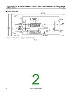
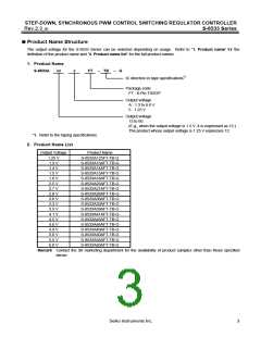
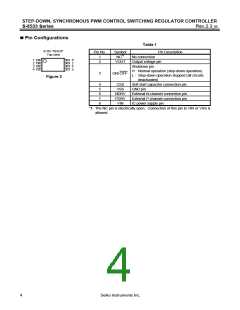
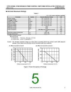
STEP-DOWN, SYNCHRONOUS PWM CONTROL SWITCHING REGULATOR CONTROLLER
S-8533 Series
Rev.2.3_00
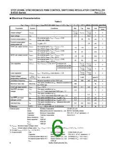
Electrical Characteristics
Table 3
VIN = VOUT × 1.5 V, IOUT = VOUT/50 A (In case VOUT ≤ 1.8 V, VIN = 2.7 V) (Ta = 25°C unless otherwise specified)
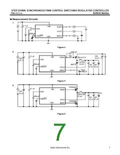
Measurement
Parameter
Symbol
Conditions
Min.
Typ.
Max.
Unit
Circuit
VOUT(S)
× 0.98
2.7
VOUT(S)
× 1.02
16.0
Output voltage*1
Input voltage
VOUT(E)
VIN
−
VOUT(S)
−
V
V
2
1
1
−
No external parts, VOUT = VOUT(S) × 0.95
(Duty ratio 100%)
Current consumption 1
ISS1
−
−
30
70
1.0
−
μA
Current consumption
during power-off
ISSS
−
μA
mA
mA
mA
mA
V
1
1
1
1
1
2
2
2
V
ON/OFF = 0 V
PDRV pin output current IPDRVH
No external parts, VOUT = VOUT(S) × 1.5,
VIN = 9.0 V, VPDRV = VIN − 0.2 V
−12
19
−10
35
−
−18
27
IPDRVL
NDRV pin output current INDRVH
INDRVL
No external parts, VOUT = VOUT(S) × 0.95,
VIN = 9.0 V, VPDRV = 0.2 V
−
No external parts, VOUT = VOUT(S) × 1.5,
VIN = 9.0 V, VNDRV = VIN − 0.2 V
−14
50
−
No external parts, VOUT = VOUT(S) × 0.95,
VIN = 9.0 V, VNDRV = 0.2 V
VIN = VOUT(S) × 1.2 to 16 V*2 S-8533A125,
−
Line regulation
ΔVOUT1
VOUT(E) VOUT(E)
× 1.0% × 2.5%
VOUT(E) VOUT(E)
× 1.0% × 2.0%
VOUT(E) VOUT(E)
× 0.5% × 1.0%
S-8533A13A to 29A
S-8533A30A to 60A
−
V
Load regulation
ΔVOUT2
IOUT = 10 μA to IOUT (see above) × 1.25
−
V
ΔVOUT
ΔTa• VOUT
Output voltage
Ta = −40 to +85°C
−
±100
300
−
−
345
−
ppm/°C
kHz
%
−
2
1
1
1
temperature coefficient
Oscillation frequency
fOSC
Measure waveform at the PDRV pin.
The same condition as lSS1. Measure waveform at
the PDRV pin.
255
100
0.01
1.8
Maximum duty ratio
MaxDuty
VOUT pin input current
IVOUT
VSH
VOUT = 5.0 V
0.1
−
4.0
−
μA
The same condition as ISS1
VIN = 2.7 V and check that PDRV pin = "L".
The same condition as ISS1
.
ON/
pin input
OFF
V
voltage
VSL
.
−
−
0.3
V
1
VIN = 16.0 V and check that PDRV pin = "H".
The same condition as ISS1. VON/OFF = VIN
The same condition as ISS1. VON/OFF = 0 V
The same condition as ISS1. Measure time until
PDRV pin oscillates.
ISH
ISL
−0.1
−0.1
−
−
0.1
0.1
μA
μA
1
1
ON/
pin input
OFF
leakage current
Soft-start time
tSS
5.0
8.0
94
16.0
ms
%
1
3
Efficiency
EFFI
*3, IOUT = 200 to 400 mA, S-8533A33A
−
−
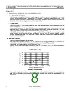
External parts :
Coil :
Sumida Corporation
CD105 (22 μH)
Diode :
Matsushita Electric Industrial Co., Ltd. MA737 (Schottky diode)
Capacitor :
Transistor :
Nichicon Corporation
Toshiba Corporation
F93 (16 V, 47 μF, tantalum) × 2
2SA1213-Y
Base resistance : 1 kΩ
Base capacitor : 2200 pF
CSS
CNDRV
*1. VOUT(S) : Nominal output voltage value
:
4700 pF
1000 pF
:
VOUT(E) : Actual output voltage value : VIN = VOUT × 1.5 V, IOUT = VOUT/50 A (If VOUT ≤ 1.8 V, VIN = 2.7 V.)
*2. In case VOUT(S) ≤ 2.2 V, VIN = 2.7 to 16 V
*3. External parts
Coil :
Sumida Corporation
Nichicon Corporation
CDRH104R (22 μH)
Capacitor :
F93 (16 V, 47 μF, tantalum) × 2
P-channel power MOS FET :
Sanyo Electric Co., Ltd. CPH6303 (VGS = 10 V max.)
N-channel power MOS FET : Sanyo Electric Co., Ltd. CPH6403 (VGS = 10 V max.)
CSS
:
4700 pF
6
Seiko Instruments Inc.

 SII [ SEIKO INSTRUMENTS INC ]