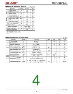
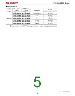
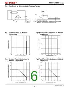
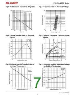
PC8171xNSZ0F Series
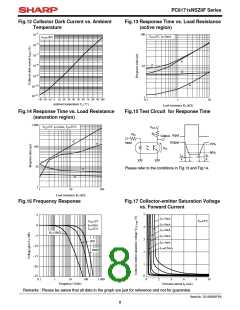
Fig.12 Collector Dark Current vs. Ambient
Temperature
Fig.13 Response Time vs. Load Resistance
(active region)
10−5
100
VCE=2V, IC=2mA
VCE=50V
10−6
10−7
10−8
10−9
tr
tf
10
td
ts
10−10
10−11
1
0.1
−30 −20 −10
0
10 20 30 40 50 60 70 80 90 100
1
10
Ambient temperature Ta (˚C)
Load resistance RL (kΩ)
Fig.14 Response Time vs. Load Resistance
(saturation region)
Fig.15 Test Circuit for Response Time
1 000
V
=5V, IF=1mA, T =25˚C
a
cc
VCC
RL
RD
Input
Input
Output
VCE
tf
Output
ts
10%
90%
100
10
ts
tf
td
tr
Please refer to the conditions in Fig.13 and Fig.14.
tr
td
1
1
10
100
Load resistance RL (kΩ)
Fig.16 Frequency Response
Fig.17 Collector-emitter Saturation Voltage
vs. Forward Current
5
5
0
IC=7mA
Ta=25˚C
IC=5mA
VCE=2V
IC=2mA
Ta=25˚C
4
IC=3mA
RL=10kΩ
−5
IC=2mA
3
1kΩ
IC=1mA
−10
−15
IC=0.5mA
100Ω
2
1
0
−20
−25
0.1
1
10
100
1 000
0
2
4
6
8
10
Frequency f (kHz)
Forward current IF (mA)
Remarks : Please be aware that all data in the graph are just for reference and not for guarantee.
Sheet No.: D2-A03302FEN
8

 SHARP [ SHARP ELECTRIONIC COMPONENTS ]