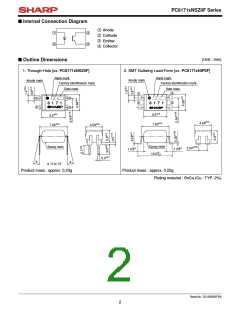
PC8171xNSZ0F Series
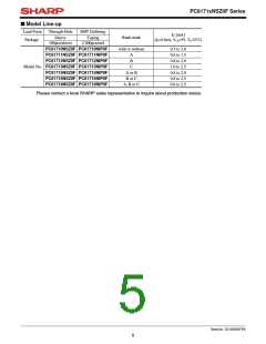
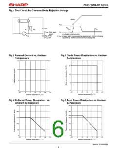
Fig.1 Test Circuit for Common Mode Rejection Voltage
(dV/dt)
VCM
1)
VCC
Vnp
Vcp
RL
Vnp
V
CM : High wave
VO
pulse
RL=470Ω
(Vcp Nearly = dV/dt×Cf×RL)
1) Vcp : Voltage which is generated by displacement current in floating
capacitance between primary and secondary side.
VCM
VCC=9V
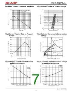
Fig.2 Forward Current vs. Ambient
Fig.3 Diode Power Dissipation vs. Ambient
Temperature
Temperature
15
15
10
10
5
0
5
0
−30
0
25
50
75
100
125
−30
0
25
50
75
100
125
Ambient temperature Ta (˚C)
Ambient temperature Ta (˚C)
Fig.4 Collector Power Dissipation vs.
Fig.5 Total Power Dissipation vs. Ambient
Ambient Temperature
250
Temperature
250
200
200
150
100
170
150
100
50
0
50
0
−30
0
25
50
75
100
125
−30
0
25
50
75
100
125
Ambient temperature Ta (˚C)
Ambient temperature Ta (˚C)
Sheet No.: D2-A03302FEN
6

 SHARP [ SHARP ELECTRIONIC COMPONENTS ]