IS471F
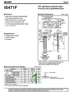
*6 Test circuit for response time, threshold irradiance is shown in Fig. 4.
Fig. 4
Vin
OFF
VCC
Light
emitting
diode
1
2
280Ω
Switch
5V
VO
ON
IS471F
tPHL
tPLH
0.33µF
Switch
GND
VOH
4
3
GLout
Output
1.5V
VOL
Light emitting diode : peak emission wavelengh λ P= 940nm
*7 E VDX : Defined as the EVD at the limit of normal operation range.
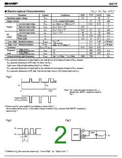
Fig. 5 Power Dissipation vs.
Fig. 6 Low Level Output Voltage vs.
Ambient Temperature
Low Level Output Current
1
300
VCC = 5V
Ta = 25˚C
0.5
250
200
150
100
0.2
0.1
0.05
50
0
0.02
0.01
- 25
0
25
50 60 75
100
125
1
2
5
10
20
50
100
(
)
(
OL
)
mA
Ambient temperature T ˚C
Low level output current I
a
Fig. 7 Low Level Output Voltage vs.
Fig. 8 Supply Current vs. Supply Voltage
Ambient Temperature
0.6
8
VCC = 5V
0.5
7
6
5
4
0.4
0.3
IOL = 30mA
0.2
16mA
3
2
0.1
5mA
0
- 25
0
25
50
75
100
0
2
4
6
8
10
12
)
14
16
(
)
(
Supply voltage Vcc V
Ambient temperature Ta ˚C

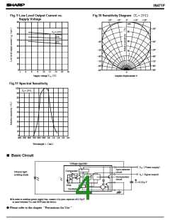
 SHARP [ SHARP ELECTRIONIC COMPONENTS ]