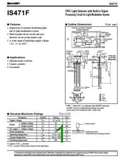
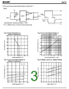
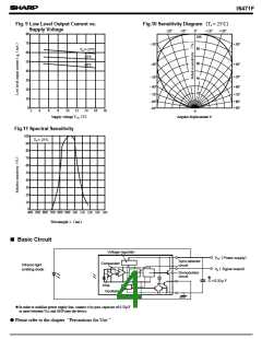
IS471F
(
)
VCC= 5V, Ta= 25˚C
■ Electro-optical Characteristics
Parameter
Operating supply voltage
Supply current
Symbol
Conditions
MIN.
4.5
-
TYP.
-
MAX.
16
Unit
VCC
ICC
V
-
VO, GL
terminals shall be opened.
3.5
0.15
-
7.0
0.35
-
mA
out
Low level output voltage
V OL
V OH
IOS
IOL= 16mA, E VP = 500lx, E VD= 0*3
EVD= EVP = 0*3
EVP = EVD= 0*3
VGL= 1.2V
-
V
Output
High level output voltage
Output short circuit current
Low level output current
*4Pulse cycle
4.97
0.25
40
70
4.4
-
V
0.5
55
1.0
70
mA
IGL
mA
GL
output
tp
130
8
220
13.7
2.66
2.8
0.95
670
670
-
µ s
-
*4Pulse width
tW
µ s
µ W/mm2
µ W/mm2
-
EeD= 0*3
*5 “Low→High ” threshold irradiance
*5 “High→Low ” threshold irradiance
E ePLH
E ePHL
0.4
0.7
0.65
400
400
7500
Light emitting
*6
-
(
)
diode
λ
p= 940nm
Hysteresis
E ePLH /E ePHL
t PHL
0.45
-
-
“ High→Low”
propagation delay time
“ Low→High”
propagation dealy time
Response
*6
*6
µ s
µ s
lx
time
t PLH
-
*7
2
External disturbing light illuminance
EVDX
Eep= 7.5 µ W/mm
,
*3 λ p= 940nm
2000
*3 EeP represents illuminance of signal light in sync with the low level timing of output at GL terminal.
out
EeD represents illuminance of DC light. For detail, see Fig. 1.
(
)
Light source: Infrared light emitting diode λ p= 940nm
EVP represents illuminance of signal light in sync with the low level timing of output at GLout terminal.
EVD represents illuminance of DC light. Note that the light source is CIE standard light source A.
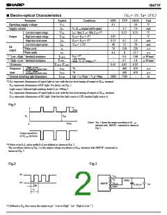
Fig.1
EeP
EeD
Ee
(
)
Note Fig. 1 shows the output waveform at GL
out
Time
0
terminal with IS471F connected as shown in
Fig. 3.
Output waveform
at GL out terminal
(
)
t P
( )
t W
are defined as shown in Fig. 2.
*4 Pulse cycle
, pulse width
The waveform shown in Fig. 2 is the output voltage waveform at GL terminal with IS471F connected as
out
shown in Fig. 3
Fig.2
Fig.3
5V
0V
VCC
VO
1
2
4
3
280Ω
GLout
GND
IS471F
5V
0.33 µF
tW
tP
(
)
.
*5 Defined as Eep that causes the output to go“ Low to High” or“ High to Low”

 SHARP [ SHARP ELECTRIONIC COMPONENTS ]