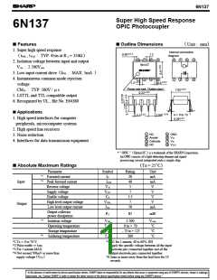
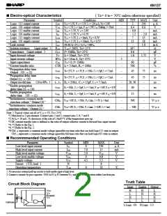
6N137
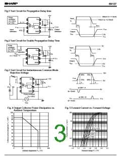
Fig.1 Test Circuit for Propagation Delay time
+5V
( )
350mV IF =7.5mA
Pulse
Input
Iin
oscillator
O = 50Ω
VCC
1
2
8
7
( )
175mV IF =3.75mA
Z
IF
t
R = 5ns
RL
tPHL
tPLH
V OUT
IF
3
4
6
5
V OH
Output
CL
Input
47Ω
detection
detection
GND
Output
Vout
1.5V
V OL
Fig.2 Test Circuit for Enable Propagation Delay Time
Pulse
oscillator
3V
+ 5V
Input
VE
Z
O = 50Ω
1.5V
Input
detection
VCC
1
2
8
7
t
R = 5ns
VE
F= 7.5mA
RL
tEHL
tELH
I
3
4
6
5
V O
V OH
CL
Output
Vout
GND
1.5V
V OL
Fig.3 Test Circuit for Instantaneous Common Mode
Rejection Voltage
10V
90%
10%
90%
V CM
VCC
+ 5V
1
2
8
7
IF
10%
0V
tr
tf
RL
V O
B
A
3
4
6
5
at SW = A
at SW = B
V O
5V
GND
(
I
)
F= 0mA
Pulse oscillator
Z
O = 50Ω
V O
V OL
( )
IF= 5mA
+
-
VCM
Fig. 4 Output Collector Power Dissipation vs.
Fig. 5 Forward Current vs. Forward Voltage
Ambient Temperature
100
100
90
85
80
10
70
60
50
40
30
20
Ta= 0˚C
1
25˚C
50˚C
70˚C
0.1
10
0
0.01
70
0
25
75
(
100
1.0
1.2
1.4
( )
Forward voltage V F V
1.6
1.8
2.0
2.2
)
Ambient temperature T ˚C
a

 SHARP [ SHARP ELECTRIONIC COMPONENTS ]