6N137
(
)
Ta= 0 to+ 70˚C unless otherwise specified
■ Electro-optical Characteristics
Parameter
Symbol
IOH
V OL
IEH
Conditions
MIN.
TYP.
2
0.4
- 0.8
- 1.2
7
13
-
1012
0.6
1.6
-
MAX.
250
0.6
-
- 2.0
15
18
1.0
Unit
µ A
V
mA
mA
mA
mA
m A
Ω
pF
V
V
pF
( )
Logic
Logic
Logic
Logic
Logic
Logic
1
output current
output voltage
enable current
enable current
supply current
supply current
VCC = 5.5V, V O = 5.5V, I F = 250
VCC = 5.5V, I F = 5mA, V
= 2.0V, I
µ
A, VE = 2.0V
-
-
-
-
-
-
-
-
-
-
5
-
-
( )
(
)
0
Sinking = 13mA
EH
OL
( )
1
VCC = 5.5V, V E = 2.0V
VCC = 5.5V, V E = 0.5V
VCC = 5.5V, I F = 0mA, VE = 0.5V
VCC = 5.5V, I F = 10mA, VE = 0.5V
45% RH, Ta = 25˚C, t = 5s, V I-O = 3 000V dc
VI-O = 500V, Ta= 25˚C
f= 1MHz, Ta= 25˚C
( )
0
IEL
( )
1
ICCH
ICCL
II-O
RI-O
CI-O
VF
( )
0
*1Leak current
*1Isolation resistance
input-output
-
-
(
)
*1Capacitance
input-output
(
)
*2Input forward voltage
Input reverse voltage
Input capacitance
IF = 10mA, Ta= 25˚C
1.75
BVR IR = 10 m A, Ta= 25˚C
CIN VF = 0, f= 1MHz
CTR IF = 5.0mA, R L = 100Ω
-
-
-
60
700
*3Current transfer ratio
*4Propagation delay time
%
t PLH
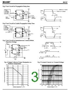
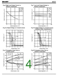
Ta = 25˚C, V CC = 5V, R L = 350Ω , C L = 15pF, I F = 7.5mA
-
45
75
ns
( )
0 → (1)
Output
*5Propagation delay time
( )
t PHL
Ta = 25˚C, V CC = 5V, R L = 350Ω , C L = 15pF, I F = 7.5mA
-
-
-
45
20, 30
40
75
-
ns
ns
ns
Output (1) →
0
(
)
Output rise-fall time
*6Enable propagation
10 to 90%
tr , t f RL = 350Ω , C L = 15pF, I F = 7.5mA
t ELH
t EHL
RL = 350Ω , C L = 15pF, I F = 7.5mA, V
RL = 350Ω , C L = 15pF, I F = 7.5mA, V
= 3.0V, V EL = 0.5V
= 3.0V, V EL = 0.5V
-
EH
EH
( )
delay time (1) →
0
*7Enable propagation
-
-
-
15
-
-
-
ns
( )
delay time
0
→ (1)
*8Instantaneous common mode
(
)
CMH V CM = 10V, R L = 350Ω , V O min. = 2V, I F = 0mA
500
V/
s
µ
( )
rejection voltage “ Output 0 ”
*8Instantaneous common mode
rejection voltage “ Output (1) ”
(
)
CML
VCM = 10V, R L = 350Ω , V
max. = 0.8V, I F = 5mA
- 500
V/ µ s
O
)
Note Typical values are all at V CC = 5V, Ta= 25˚C
*1 Measured as 2-pin element. Connect pins 2 and 3, connect pins 5, 6, 7 and 8.
*2 At Iin = 10 mA, VF decreases at the rate of 1.6mV/˚C if the temperature goes up.
*3 DC current transfer ratio is defined as the ratio of output collector current to forward bias input current.
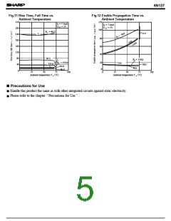
*4, *5 Refer to the Fig. 1.
*6, *7 Refer to the Fig. 2.
(
)
*8 CM represents a common mode voltage ignorable rise time ratio that can hold logic 1 state in output.
H
(
)
CM represents a common mode voltage ignorable fall time ratio that can hold logic 0 state in output.
L
■ Recommmended Operating Conditions
Parameter
Low level input current
High level input current
High level enable voltage
Low level enable voltage
Supply voltage
Symbol
IFL
IFH
V EH
V EL
VCC
N
MIN.
0
7.0
2.0
0
MAX.
250
15
VCC
0.8
5.5
8
Unit
µ A
mA
V
V
V
4.5
-
(
)
Fanout
TTL load
-
Operating temperature
T opr
0
70
˚C
1. No necessary external pull-up resistor to hold enable input at high level
(
)
2. Connect a ceramic by-pass capacitor 0.01 to 0.1
µ
F
between VCC and GND at the position within 1cm from pin.
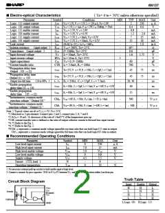
Truth Table
Circuit Block Diagram
Input
Enable
Output
V
V
CC
E
H
L
H
H
H
L
L
L
H
H
H
Anode
(
)
Enable
O
V
L
Cathode
(
)
( )
H:Logic 1
L:Logic
0
GND

 SHARP [ SHARP ELECTRIONIC COMPONENTS ]