SX1231
ADVANCED COMMUNICATIONS & SENSING
DATASHEET
5.2. Control Block Description
5.2.1. SPI Interface
The SPI interface gives access to the configuration register via a synchronous full-duplex protocol corresponding to CPOL
= 0 and CPHA = 0 in Motorola/Freescale nomenclature. Only the slave side is implemented.
Three access modes to the registers are provided:
SINGLE access: an address byte followed by a data byte is sent for a write access whereas an address byte is sent and
a read byte is received for the read access. The NSS pin goes low at the begin of the frame and goes high after the data
byte.
BURST access: the address byte is followed by several data bytes. The address is automatically incremented internally
between each data byte. This mode is available for both read and write accesses. The NSS pin goes low at the
beginning of the frame and stay low between each byte. It goes high only after the last byte transfer.
FIFO access: if the address byte corresponds to the address of the FIFO, then succeeding data byte will address the
FIFO. The address is not automatically incremented but is memorized and does not need to be sent between each data
byte. The NSS pin goes low at the beginning of the frame and stay low between each byte. It goes high only after the
last byte transfer.
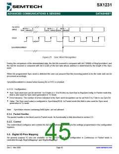
Figure below shows a typical SPI single access to a register.
Figure 22. SPI Timing Diagram (single access)
MOSI is generated by the master on the falling edge of SCK and is sampled by the slave (i.e. this SPI interface) on the
rising edge of SCK. MISO is generated by the slave on the falling edge of SCK.
A transfer always starts by the NSS pin going low. MISO is high impedance when NSS is high.
The first byte is the address byte. It is made of:
wnr bit, which is 1 for write access and 0 for read access
7 bits of address, MSB first
The second byte is a data byte, either sent on MOSI by the master in case of a write access, or received by the master on
MISO in case of read access. The data byte is transmitted MSB first.
Proceeding bytes may be sent on MOSI (for write access) or received on MISO (for read access) without rising NSS and
re-sending the address. In FIFO mode, if the address was the FIFO address then the bytes will be written / read at the
FIFO address. In Burst mode, if the address was not the FIFO address, then it is automatically incremented at each new
byte received.
Rev 2 - Nov 2009
Page 42
www.semtech.com

 SEMTECH [ SEMTECH CORPORATION ]