SX1231
ADVANCED COMMUNICATIONS & SENSING
DATASHEET
5. Data Processing
5.1. Overview
5.1.1. Block Diagram
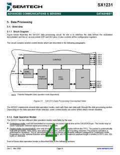
Figure below illustrates the SX1231 data processing circuit. Its role is to interface the data to/from the modulator/
demodulator and the uC access points (SPI and DIO pins). It also controls all the configuration registers.
The circuit contains several control blocks which are described in the following paragraphs.
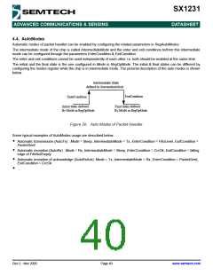
DIO0
Tx/Rx
DIO1
DIO2
DIO3
DIO4
DIO5
CONTROL
Data
Rx
Tx
SYNC
RECOG.
PACKET
HANDLER
FIFO
(+SR)
SPI
NSS
SCK
MOSI
MISO
Potential datapaths (data operation mode dependant)
Figure 21. SX1231 Data Processing Conceptual View
The SX1231 implements several data operation modes, each with their own data path through the data processing section.
Depending on the data operation mode selected, some control blocks are active whilst others remain disabled.
5.1.2. Data Operation Modes
The SX1231 has two different data operation modes selectable by the user:
Continuous mode: each bit transmitted or received is accessed in real time at the DIO2/DATA pin. This mode may be
used if adequate external signal processing is available.
Packet mode (recommended): user only provides/retrieves payload bytes to/from the FIFO. The packet is automatically
built with preamble, Sync word, and optional AES, CRC, and DC-free encoding schemes The reverse operation is
performed in reception. The uC processing overhead is hence significantly reduced compared to Continuous mode.
Depending on the optional features activated (CRC, AES, etc) the maximum payload length is limited to FIFO size, 255
bytes or unlimited.
Each of these data operation modes is described fully in the following sections.
Rev 2 - Nov 2009
Page 41
www.semtech.com

 SEMTECH [ SEMTECH CORPORATION ]