SX1231
ADVANCED COMMUNICATIONS & SENSING
DATASHEET
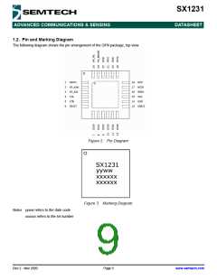
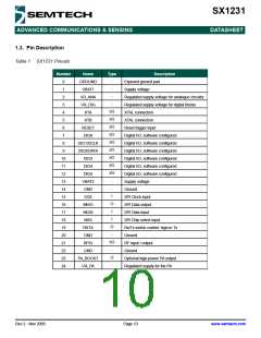
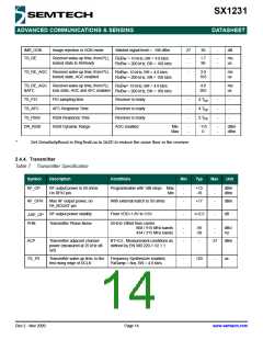
1.3. Pin Description
Table 1 SX1231 Pinouts
Number
0
Name
GROUND
VBAT1
VR_ANA
VR_DIG
XTA
Type
Description
Exposed ground pad
-
-
-
1
Supply voltage
2
Regulated supply voltage for analogue circuitry
Regulated supply voltage for digital blocks
XTAL connection
-
3
I/O
I/O
I/O
I/O
I/O
I/O
I/O
I/O
I/O
-
4
5
XTB
XTAL connection
6
RESET
DIO0
Reset trigger input
7
Digital I/O, software configured
Digital I/O, software configured
Digital I/O, software configured
Digital I/O, software configured
Digital I/O, software configured
Digital I/O, software configured
Supply voltage
8
DIO1/DCLK
DIO2/DATA
DIO3
9
10
11
12
13
14
15
16
17
18
19
20
21
22
23
24
DIO4
DIO5
VBAT2
GND
-
Ground
I
SCK
SPI Clock input
O
I
MISO
SPI Data output
MOSI
SPI Data input
I
NSS
SPI Chip select input
Rx/Tx switch control: high in Tx
Ground
O
-
RXTX
GND
I/O
-
RFIO
RF input / output
GND
Ground
O
-
PA_BOOST
VR_PA
Optional high-power PA output
Regulated supply for the PA
Rev 2 - Nov 2009
Page 10
www.semtech.com

 SEMTECH [ SEMTECH CORPORATION ]