SX1232
WIRELESS & SENSING
DATASHEET
Name
(Address)
Default
value
Bits
Mode
Variable Name
Description
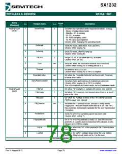
RegDioMapping1 7-6
Dio0Mapping
Dio1Mapping
Dio2Mapping
Dio3Mapping
Dio4Mapping
Dio5Mapping
reserved
rw
rw
rw
rw
rw
rw
rw
rw
0x00
0x00
0x00
0x00
0x00
0x00
(0x40)
5-4
Mapping of pins DIO0 to DIO5
3-2
1-0
See Table 27 for mapping in Continuous mode
See Table 28 for mapping in Packet mode
RegDioMapping2 7-6
(0x41)
5-4
3-1
0
0x00 reserved. Retain default value
MapPreambleDetect
0x00 Allows the mapping of either Rssi Or PreambleDetect to the
DIO pins, as summarized on Table 27 and Table 28
0 Æ Rssi interrupt
1 Æ PreambleDetect interrupt
Version register
RegVersion
(0x42)
7-0
Version
r
0x21 Version code of the chip. Bits 7-4 give the full revision number;
bits 3-0 give the metal mask revision number.
Additional registers
RegAgcRef
(0x43)
7-6
5-0
unused
r
-
unused
AgcReferenceLevel
rw
0x13 Sets the floor reference for all AGC thresholds:
AGC Reference[dBm]=
-174dBm+10*log(2*RxBw)+SNR+AgcReferenceLevel
SNR = 8dB, fixed value
RegAgcThresh1
(0x44)
7-5
4-0
7-4
3-0
7-4
3-0
7
unused
AgcStep1
AgcStep2
AgcStep3
AgcStep4
AgcStep5
FastHopOn
r
-
unused
rw
rw
rw
rw
rw
rw
0x0e Defines the 1st AGC Threshold
0x05 Defines the 2nd AGC Threshold:
0x0b Defines the 3rd AGC Threshold:
0x0d Defines the 4th AGC Threshold:
0x0b Defines the 5th AGC Threshold:
RegAgcThresh2
(0x45)
RegAgcThresh3
(0x46)
RegPllHop
(0x4b)
0x00 Bypasses the main state machine for a quick frequency hop.
Writing RegFrfLsb will trigger the frequency change.
0 Æ Frf is validated when FSTx or FSRx is requested
1 Æ Frf is validated triggered when RegFrfLsb is written
6-0
7-5
4
reserved
reserved
rw
rw
rw
0x2e reserved
RegTcxo
(0x58)
0x00 reserved. Retain default value
TcxoInputOn
0x00 Controls the crystal oscillator
0 Æ Crystal Oscillator with external Crystal
1 Æ External clipped sine TCXO AC-connected to XTA pin
3-0
7-3
2-0
reserved
reserved
PaDac
rw
rw
rw
0x09 Reserved. Retain default value.
0x10 reserved. Retain default value
RegPaDac
(0x5a)
0x04 Enables the +20dBm option on PA_BOOST pin
0x04 Æ Default value
0x07 Æ +20dBm on PA_BOOST when OutputPower=1111
Rev 3 - August 2012
Page 79
www.semtech.com

 SEMTECH [ SEMTECH CORPORATION ]