SX1232
WIRELESS & SENSING
DATASHEET
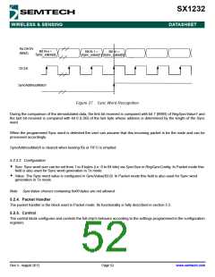
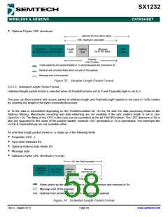
5.4. Continuous Mode
5.4.1. General Description
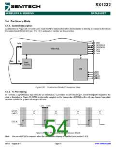
As illustrated in Figure 28, in Continuous mode the NRZ data to (from) the (de)modulator is directly accessed by the uC on
the bidirectional DIO2/DATA pin. The FIFO and packet handler are thus inactive.
DIO0
Tx/Rx
DIO1/DCLK
DIO2/DATA
DIO3
CONTROL
DIO4
DIO5
Data
Rx
SYNC
RECOG.
SPI
NSS
SCK
MOSI
MISO
Figure 28. Continuous Mode Conceptual View
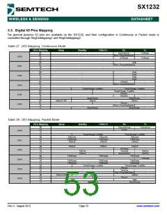
5.4.2. Tx Processing
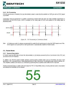
In Tx mode, a synchronous data clock for an external uC is provided on DIO1/DCLK pin. Clock timing with respect to the
data is illustrated in Figure 29. DATA is internally sampled on the rising edge of DCLK so the uC can change logic state
anytime outside the grayed out setup/hold zone.
T_DATA
T_DATA
DATA
(NRZ)
DCLK
Figure 29. Tx Processing in Continuous Mode
Note the use of DCLK is required when the modulation shaping is enabled (see section 3.4.5).
Rev 3 - August 2012
Page 54
www.semtech.com

 SEMTECH [ SEMTECH CORPORATION ]